ADN4697E_ Просмотр технического описания (PDF) - Analog Devices
Номер в каталоге
Компоненты Описание
производитель
ADN4697E_ Datasheet PDF : 12 Pages
| |||
AN-1177
Application Note
JITTER, SKEW, DATA ENCODING, AND SYNCHRONIZATION
With high speed differential signaling, such as LVDS and
M-LVDS, accurate timing is critical to the performance of a
system. PCB traces, connectors, and cabling can degrade the
performance of data and clock signals, requiring that a margin
for error is also present in system timing. This means that
careful timing analysis may be required to achieve the maxi-
mum throughput on an LVDS or M-LVDS communication link.
Modern FPGAs and processors also have built-in capabilities to
correct for timing errors, although there may be clearly defined
limits to the amount of jitter tolerated, for example.
WHAT IS JITTER?
Jitter refers to the apparent movement of a signal edge with
respect to the ideal time position of that signal edge. If a
periodic signal is observed on an oscilloscope, the edges
literally jitter back and forth with respect to the reference point.
one type of deterministic jitter and refers to the time difference
between each cycle compared to the ideal. Periodic jitter is also
recorded as a peak-to-peak value, that is, the difference between
the longest and shortest periods observed
WHAT IS SKEW?
There are different definitions for skew, several of which are
typically considered in designing high speed LVDS links. The
most basic definition of skew is the difference in propagation
time between the two signals in a differential pair. This means
that edge transitions on one signal in a pair will not match up
exactly with transitions on the complementary signal (the
crossover will be asymmetric).
D–
INPUT
IDEAL
TIE
ACTUAL
(ONE
PASS)
ACTUAL
(MULTIPLE
PASSES)
EYE
JITTER
(PEAK-
TO-PEAK)
Figure 16. Waveforms Showing Time Interval Error, Jitter and Eye
Jitter can be quantified simply as time interval error, the time
difference between when a signal edge occurs, and when it
should occur. Usually in order to determine the sources of
jitter, a large number of TIE samples are recorded to build a
histogram, from which deterministic jitter can be separated
from random jitter. Total jitter can be quantified as a peak-to-
peak value when bounded to a specific quantity of samples.
The peak-to-peak value means the time difference between
the earliest and latest edge observed during sampling.
Peak-to-peak jitter can be seen visually if multiple waveform
samples are overlaid on an oscilloscope display (infinite
persistence), as shown in Figure 16. The width of the overlaid
transitions is the peak-to-peak jitter, with the clear area in-
between referred to as the eye. This eye is the area available for
sampling by a receiver.
Random jitter occurs due to noise, both electrical and thermal.
The result is a Gaussian distribution to the time error, with this
error introduced as random jitter. The jitter is unbounded;
when more samples are recorded, the probability function
continues to grow.
Deterministic jitter is, by contrast, bounded. There is a fixed
amount of this jitter in the system due to specific factors, such
as the board layout and driver performance. Periodic jitter is
D+
IDEAL
OUTPUT
tPLH = tPHL
ACTUAL
OUTPUT
tPLH
D–
D+
tPHL
D–
D+
PULSE SKEW
(tPHL – tPLH)
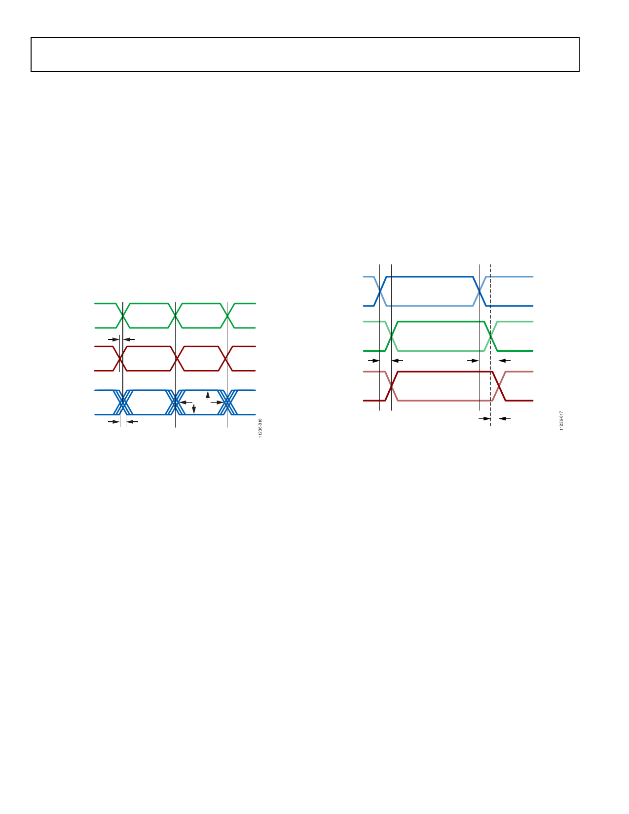
Figure 17. Waveforms Illustrating Pulse Skew Calculation
Pulse skew on a differential signal refers to the difference
between the low-to-high transition time (tPLH) and the high-to-
low transition time (tPHL). This results in duty cycle distortion,
that is, the bit period is longer or shorter for a Logic 1 or Logic 0.
Pulse skew is illustrated in Figure 17. The blue waveform
corresponds to an input signal, the green waveform to an ideal
output (where propagation times on high-to-low and low-to-
high transitions are matched), and the red waveform to an
actual output, where the difference between tPLH and tPHL results
in pulse skew.
Channel-to-channel skew and part-to-part skew are some of
the most important parameters in typical LVDS applications
because they have multiple data channels that need to remain
synchronized. Channel-to-channel skew refers to the difference,
across all channels in a part, between the fastest and slowest
low-to-high transition, or the fastest and slowest high-to-low
transition (whichever is larger). Part-to-part skew extends this
concept to channels across multiple parts.
Skew across multiple channels (on one or multiple parts) is
illustrated in Figure 18. The blue waveform corresponds to an
input signal, with the four red waveforms comprising output
channels on one or more parts. The difference between the
fastest and slowest tPLH is calculated, along with the difference
between the fastest and slowest tPHL. The channel-to-channel or
Rev. 0 | Page 8 of 12
Share Link: 