ADN4693E_ Просмотр технического описания (PDF) - Analog Devices
Номер в каталоге
Компоненты Описание
производитель
ADN4693E_ Datasheet PDF : 12 Pages
| |||
Application Note
TERMINATION AND PCB LAYOUT
High speed communication links, such as those used for LVDS
and M-LVDS, should be considered in the context of trans-
mission line theory, whether cables or PCB traces are used. The
high data rates of LVDS and M-LVDS require fast rise times,
meaning that impedance discontinuities and the end of the
communication link can significantly affect the transmitted
signal as it propagates from the driver to the far ends of the bus.
To avoid degradation of the signal, controlled impedances along
the communication medium, as well as proper termination, are
required.
D+
Z0
R+
Tx
Rx
RT
DRIVER
D–
Z0
R– RECEIVER
Z0 = RT (TERMINATION MATCHES CABLE/TRACK IMPEDANCE)
Figure 14. Point-to-Point Termination
The termination resistor should match the impedance of the
communication medium; for LVDS, this is usually 100 Ω. For a
simple point-to-point link, it is only necessary to terminate the
end of the bus furthest from the driver, as shown in Figure 14.
For multi-drop buses, the same termination can be used if the
driver is at one end of the bus. Otherwise, both ends of the bus
need to be terminated.
With M-LVDS, both ends of the bus are terminated, and the
drivers are designed with increased drive strength, partly to
accommodate the double termination (the effective load is
50 Ω rather than 100 Ω).
Some devices have built-in termination. This termination may
need to be disabled if the device is located at the wrong point
on the bus for termination, or if there is already proper
termination on the bus. If there are two or more 100 Ω resistors
for LVDS, or more than two for M-LVDS, then the bus is over-
terminated. This results in reduced signal amplitude and
increased reflections, combining to decrease noise immunity,
degrade timing accuracy and reducing the maximum
transmission distance.
CONTROLLED IMPEDANCES
One difficulty in LVDS and M-LVDS links is providing a
consistent controlled impedance across the bus. For links across
a single PCB, impedance discontinuities can easily arise from
vias, mismatches in trace lengths between each signal in a
differential pair, and changes in the spacing between tracks, or
the size of tracks.
For differential signaling on a PCB, the two signal traces are
usually placed close together and tightly coupled. This means
that the signals have a common field, cancelling emissions and
AN-1177
reducing susceptibility to common-mode noise. One difficulty
that arises is that if the traces need to move apart, for example,
to reach a connector, then a change in impedance between the
signals is introduced. It can be preferable to relax how closely
the signals are coupled, but maintain consistent spacing and
track thickness across the entire link.
Sharp turns or a series of bends in the PCB traces can also affect
the signal quality. Generally, turns in the PCB traces should be
minimized and kept to 45-degree angles (ideally with curves
rather than sharp angles).
Skew can be introduced between the two signals in a differential
pair if one signal follows a longer trace than the other does. It
may not always be possible to have traces exactly the same
length, but PCB layout should attempt to keep the trace lengths
matched.
Connectors should be chosen to minimize any difference in
impedance that they present on a bus, and cables or backplanes
should also match the impedance of PCB traces where possible.
Backplane connections can add significant capacitance to the
bus and it may be necessary to reduce the data rate or PCB
trace distances to allow for any degradation of the data signal
that occurs.
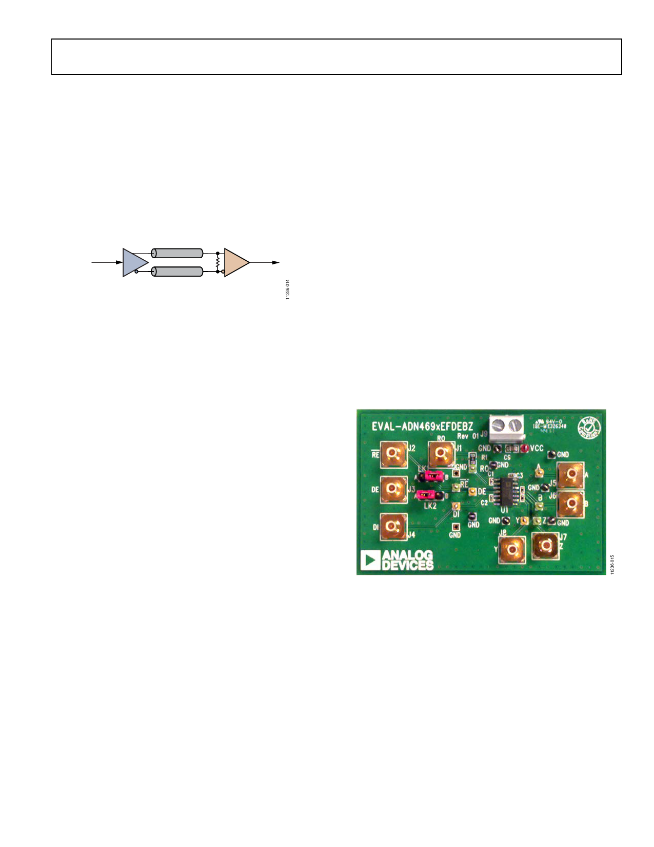
Figure 15. EVAL-ADN469xEFDEBZ Customer Evaluation Board
An example high speed PCB layout for M-LVDS is shown
in Figure 15, the EVAL-ADN469xEFDEBZ evaluation board
for full-duplex ADN469xE family M-LVDS transceivers.
Track lengths on A, B, Y, and Z are matched and have a
50 Ω impedance created using a 4-layer board layout. The
termination resistor placement is next to the device pins. The
circuit does not fully correspond to an application layout
because there are additional components, such as test points
and jumper options.
Rev. 0 | Page 7 of 12
Share Link: 