ADN4697E_ Просмотр технического описания (PDF) - Analog Devices
Номер в каталоге
Компоненты Описание
производитель
ADN4697E_ Datasheet PDF : 12 Pages
| |||
AN-1177
Application Note
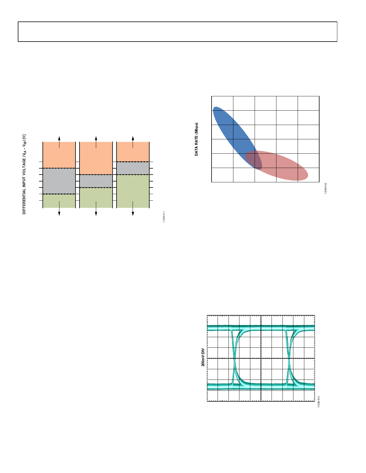
For Type 1 M-LVDS receivers, a positive VOD ≥ +50 mV
corresponds to a Logic 1 and a negative VOD ≤ −50 mV
corresponds to a Logic 0.
In between these voltage thresholds is the transition region.
If an input signal remains at a voltage level between the
thresholds, the receiver output is undefined under LVDS; it
can be high or low. This can occur if no active LVDS driver is
connected to the receiver, or if there is a short circuit. Analog
Devices LVDS receivers incorporate a failsafe feature, so that in
these cases, the receiver output is high.
LVDS
RECEIVER
OUTPUT
M-LVDS TYPE 1
RECEIVER
OUTPUT
M-LVDS TYPE 2
RECEIVER
OUTPUT
(depending on the cable type). M-LVDS can generally be
transmitted across longer cables due to the increased driver
strength, but data rates of hundreds of Mbps require shorter
cables than data rates of only tens of Mbps. Figure 12 provides
a general indication of the combinations of LVDS and M-LVDS
data rates and cable lengths typical for some applications.
1200
1000
800
LVDS
600
0.15
0.10
0.05
0
–0.05
–0.10
–0.15
LOGIC 1
UNDEFINED*
LOGIC 0
LOGIC 1
UNDEFINED
LOGIC 0
LOGIC 1
UNDEFINED
LOGIC 0
0.15
0.10
0.05
0
–0.05
–0.10
–0.15
*LOGIC 1 FOR LVDS RECEIVERS WITH FAILSAFE
Figure 11. Receiver Thresholds for LVDS and M-LVDS
With M-LVDS, any node on the bus can transmit, but when
no node is active, all driver outputs are disabled. As with LVDS,
this results in a differential output voltage in the undefined
region for Type 1 receivers. In order to provide a failsafe
condition, M-LVDS defines Type 2 receivers that have an
offset receiver threshold of >= +150 mV for a logic high and
<= +50 mV for a logic low. This means that the failsafe output
from Type 2 M-LVDS receivers is a logic low. Receiver
thresholds are shown in Figure 11 for LVDS receivers, M-LVDS
Type 1 receivers and M-LVDS Type 2 receivers.
TRANSMISSION DISTANCE
Both LVDS and M-LVDS transmission distances are affected by
two main factors: the transmission medium and the data rate.
The standard deciding factor of whether a given transmission
distance is practical, is how much jitter is observed by receiving
nodes. This is application dependent; some applications require
5% or less jitter, whereas others tolerate up to 20%.
PCB traces typically allow transmission distances on the order
of tens of centimeters, whereas twisted pair cable allows
transmission on the order of meters for LVDS or tens of meters
for M-LVDS. Different specifications of PCB construction or
cable types affect the signal differently and thus have an impact
on the maximum transmission distance.
Higher data rates greatly constrain the transmission distance;
LVDS at 1 Gbps might only be transmitted across high-quality
cables of 1 meter (possibly with additional signal conditioning),
but at 100 Mbps may be transmitted across 10 meters
400
M-LVDS
200
0
0
5
10
15
20
25
CABLE LENGTH (m)
Figure 12. Cable Length (Twisted-Pair) vs. Data Rate for Some Typical LVDS
and M-LVDS Applications
Other factors influencing the maximum distance include:
• The transmitter specifications.
• Other transmission medium components, such as vias (on
PCB traces) or connectors for cables.
• For M-LVDS or multi-drop LVDS, the number of nodes on
the bus and the stub lengths.
TIA/EIA-644 (LVDS) and TIA/EIA-899 (M-LVDS) recommend
testing intended cable lengths in the application if possible, due
to the multiple factors involved that affect the possible cable
length. This allows the jitter on the received signal to be
measured, providing a guide as to how practical a given cable
type and length is. Measurements can be taken using an eye
diagram; the ADN4696E driver output is shown in Figure 13.
1ns/DIV
Figure 13. ADN4696E Driver Output Eye Diagram
Rev. 0 | Page 6 of 12
Share Link: 