M54676E Просмотр технического описания (PDF) - MITSUBISHI ELECTRIC
Номер в каталоге
Компоненты Описание
производитель
M54676E Datasheet PDF : 5 Pages
| |||
MITSUBISHI <CONTROL / DRIVER IC>
M54676P
2-PHASE STEPPER MOTOR DRIVER
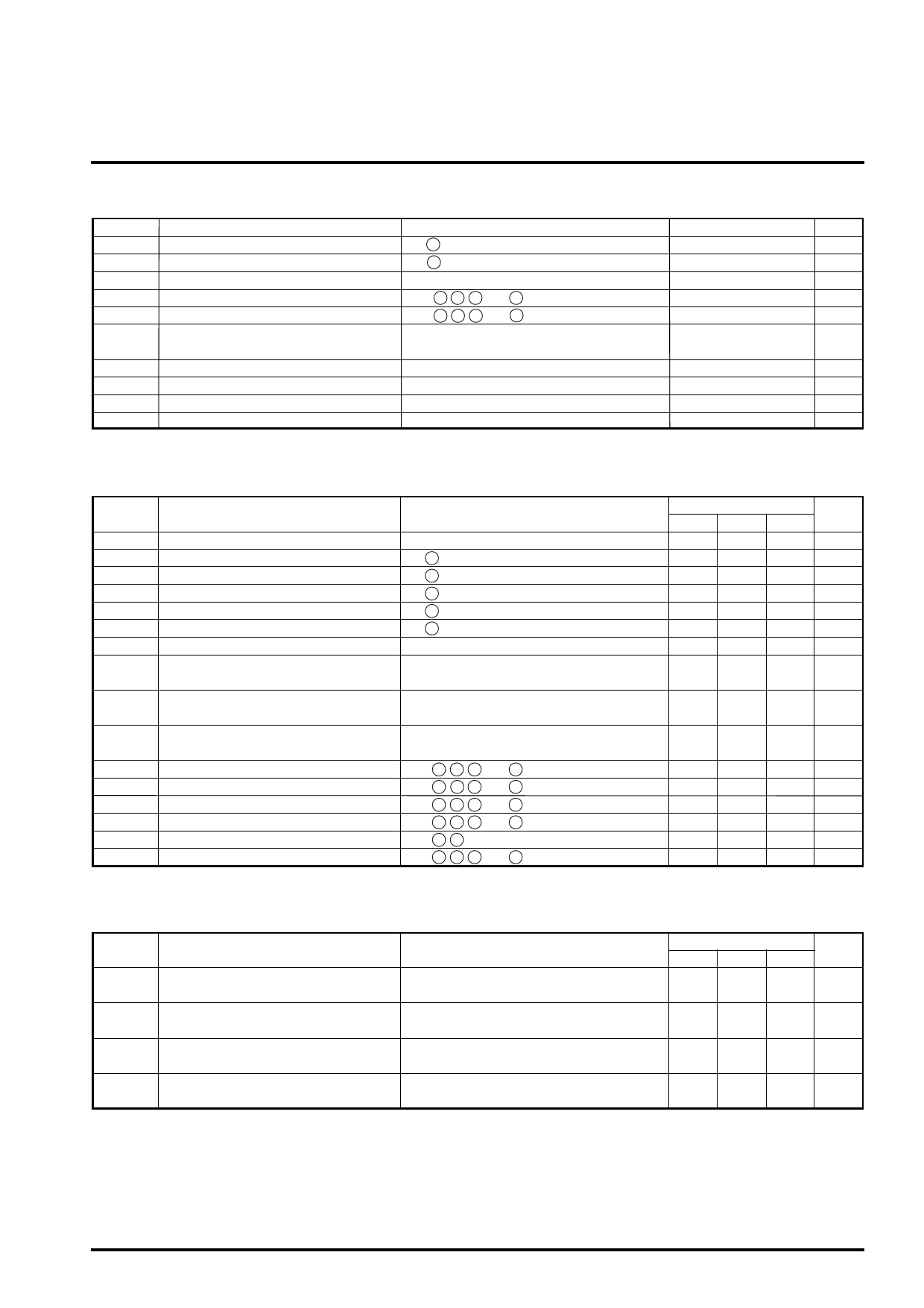
ABSOLUTE MAXIMUM RATINGS (Ta= 25˚C, unless otherwise noted)
Symbol
VM
Vcc5
Iout
Vanalg
Vlogic
Parameter
Supply voltage 1
Supply voltage 2
Maximum output current
Analog input voltage
Logic input voltage
Pt
Allowable loss
Kθ
Thermal derating
Tj
Junction temperature
Ta
Operating temperature
Tstg
Storage temperature
Pin 20
Pin 10
Conditions
Pins 4 7 13 and 14
Pins 8 9 11 and 12
100mm x 100mm, t=1.6mm
Glass epoxy board (θ ja=50˚C/W )
ditto
Ratings
Vcc5 – 20
-0.3 – 7
±500
-0.3 – 7
-0.3 – 7
2.5
20.0
150
0 – 75
-20 – 125
Unit
V
V
mA
V
V
W
mW/˚C
˚C
˚C
˚C
ELECTRICAL CHARACTERISTICS (DC CHARACTERISTICS) (Ta=25˚C, VM=12V, Vcc=5V, unless otherwise noted)
Symbol
Parameter
Vsat
Vcc5 H
Vcc5 L
Icc10
Icc20
Istby
Ivref
Output saturation voltage
Vcc5 input voltage H
Vcc5 input voltage L
Circuit current
VM reactive current
Standby VM current
Vref input bias current
Vref
Vref amplifier input voltage range
Vsense Sense pin threshold voltage
Test conditions
Load=350mA (total)
Pin 10 (Vcc5) voltage (Operating mode)
Pin 10 (Vcc5) voltage (Standby mode)
Pin 10 current (Vcc5=5V)
Pin 20 current (VM=12V, Vcc5=5V)
Pin 20 current (VM=12V, Vcc5=0V)
Vref=0V
See Vref-Vsense characteristics 12-4
Vcoff : Comparator OFF reference voltage
Sense pin voltage when output changes at
Vref=2.5V
Limits
Unit
Min. Typ. Max.
1.35 1.8
V
4.5 5.0 5.5
V
0
0.8
V
38
57
mA
6
20
mA
0
100
µA
-200 -10
nA
Vcc off
Vcc5
-1.5
V
230 250 270 mV
Vcoff
Comparator OFF reference voltage
0.1 0.2 0.3
V
Vin H
Vin L
Iin H
Iin L
Isense
Ioff
Logic input voltage H
Logic input voltage L
Logic input current H
Logic input current L
Sense input current
Output cutoff current
Pins 8 9 11 and 12
Pins 8 9 11 and 12
Pins 8 9 11 and 12 =5V
Pins 8 9 11 and 12 =0V
Pins 4 14 =0V
Pins 1 2 11 and 12
2.0
Vcc5 V
0
0.8
V
0
10
µA
-20
-7
µA
-15
-2
µA
0
100
µA
ELECTRICAL CHARACTERISTICS (AC CHARACTERISTICS) (Ta=25˚C, VM=12V, Vcc=5V, unless otherwise noted)
Symbol
Parameter
Tdon
Output turn-on delay
Test conditions
Time required to turn on output when Sense pin
voltage is decreased from 0.5V to 0V at Vref=2.5V
Limits
Min. Typ. Max. Unit
0.3
1.0
µS
Tdoff
Output turn-off delay
Time required to turn off output when Sense pin
voltage is increased from 0V to 0.5V at Vref=2.5V
1.5
2.5
µS
Tdamp Vref amplifier response time
Time required to turn on output when Vref pin voltage
is increased from 0V to 3.5V at Sense=0.25V
10
30
µS
Tdph
Phase delay time
Time required to turn on output when Phase pin voltage is
increased from 0V to 5V at Vref=2.5V and Sense=0V
Tdoff
Tdon
3
12
µS
Share Link: 