ISL9016 Просмотр технического описания (PDF) - Renesas Electronics
Номер в каталоге
Компоненты Описание
производитель
ISL9016 Datasheet PDF : 11 Pages
| |||
ISL9016
Absolute Maximum Ratings
VIN to GND . . . . . . . . . . . . . . . . . . . . . . . . . . . . . . . . . . . . . . . . . -0.3V to +7.1V
All Other Pins to GND . . . . . . . . . . . . . . . . . . . . . . . . . . . . -0.3 to (VIN + 0.3)V
Recommended Operating Conditions
Supply Voltage (VIN) . . . . . . . . . . . . . . . . . . . . . . . . . . . . . . . . . . . 1.8V to 6.5V
Each LDO Load Current . . . . . . . . . . . . . . . . . . . . . . . . . . . . . . . up to 150mA
Ambient Temperature Range (TA) . . . . . . . . . . . . . . . . . . . . -40°C to +85°C
Thermal Information
Thermal Resistance
JA (°C/W)
6 Ld µTDFN Package (Note 5) . . . . . . . . . . . . . . . . . . . .
117.5
Junction Temperature Range . . . . . . . . . . . . . . . . . . . . . . .-40°C to +125°C
Operating Temperature Range . . . . . . . . . . . . . . . . . . . . . . -40°C to +85°C
Storage Temperature Range. . . . . . . . . . . . . . . . . . . . . . . .-65°C to +150°C
Pb-Free Reflow Profile . . . . . . . . . . . . . . . . . . . . . . . . . . . . . . . see link below
http://www.intersil.com/pbfree/Pb-FreeReflow.asp
CAUTION: Do not operate at or near the maximum ratings listed for extended periods of time. Exposure to such conditions may adversely impact product
reliability and result in failures not covered by warranty.
NOTE:
5. JA is measured in free air with the component mounted on a high effective thermal conductivity test board with “direct attach” features. See Tech
Brief TB379.
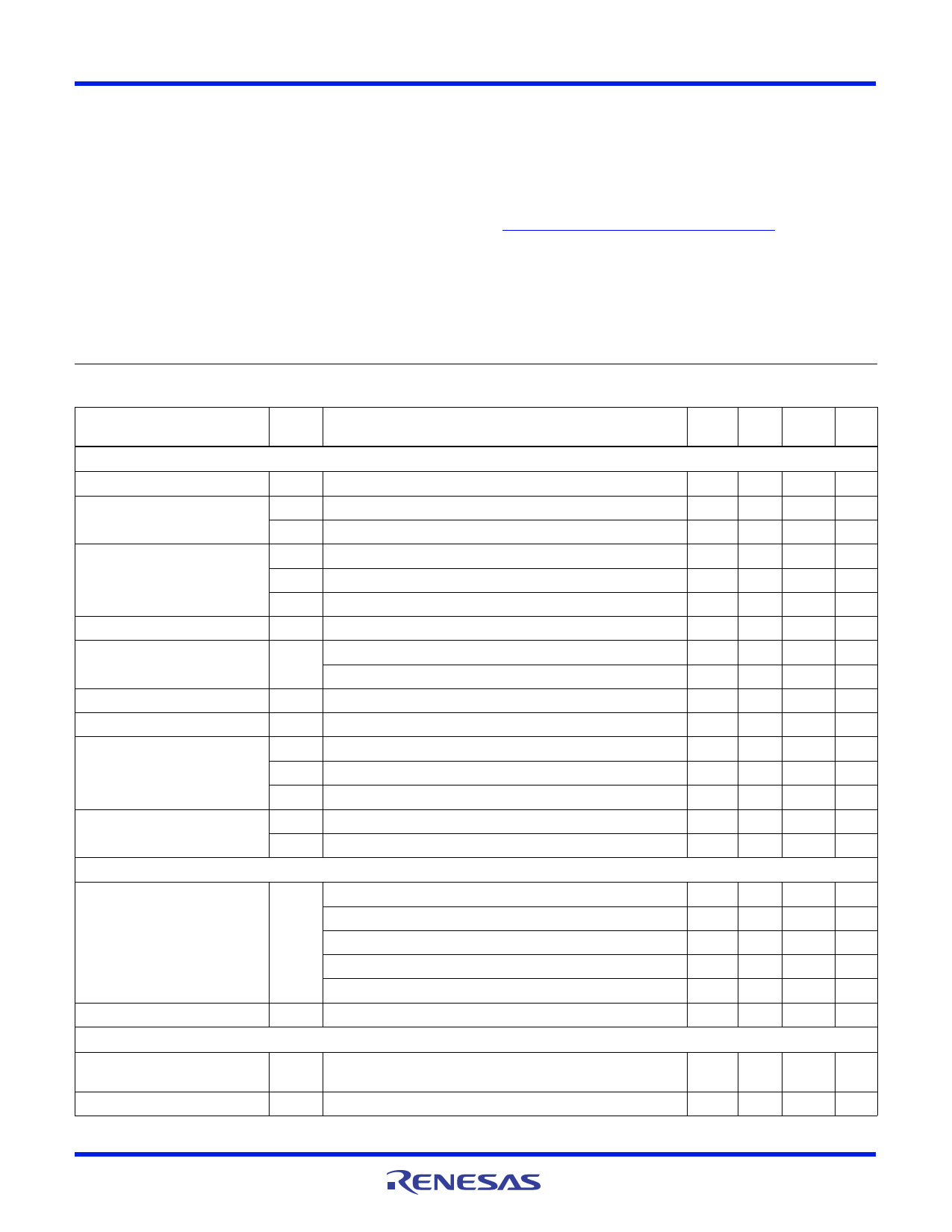
Electrical Specifications Typical specifications are measured at the following conditions: TA = +25°C; VIN = (VO + 0.5V) to 6.5V with a
minimum VIN of 1.8V; CIN = 1µF; CO = 1µF. Boldface limits apply over the operating temperature range, -40°C to +85°C.
PARAMETER
SYMBOL
TEST CONDITIONS
MIN
MAX
(Note 8) TYP (Note 8) UNITS
DC CHARACTERISTICS
Supply Voltage
UVLO Threshold
Input Quiescent Current
Shutdown Current
Regulation Voltage Accuracy
Maximum Output Current
Internal Current Limit
Dropout Voltage (Note 6)
Thermal Shutdown Temperature
AC CHARACTERISTICS
VIN
1.8
6.5
V
VUV+
1.710 1.775 V
VUV-
1.55 1.62
Quiescent condition: IO1 = 0µA; IO2 = 0µA
IDD1 One LDO active
49
67
µA
IDD2 Both LDO active
80 100 µA
IDDS @ +25°C
0.1 1.0 µA
VIN = VO + 0.5V to 6.5V, IO = 10µA to 150mA, TA = +25°C
-0.8
+0.8 %
VIN = VO + 0.5V to 6.5V, IO = 10µA to 150mA, TA = -40°C to +85°C -1.8
+1.8 %
IMAX Each LDO, Continuous
150
mA
ILIM
175 265 355 mA
VDO1 IO = 150mA; 1.2V VO 2.1V
250 425 mV
VDO2 IO = 150mA; 2.1V VO 2.8V
200 325 mV
VDO3 IO = 150mA; 2.8V VO
120 200 mV
TSD+
145
°C
TSD-
110
°C
Ripple Rejection
IO = 10mA, VIN = 3.7V(min), VO = 2.7V, TA = +25°C
@ 1kHz
80
dB
@ 10kHz
60
dB
@ 100kHz
50
dB
@ 1MHz
45
dB
Output Noise Voltage
DEVICE START-UP CHARACTERISTICS
VIN = 4.2V, IO = 10mA, TA = +25°C, BW = 10Hz to 100kHz
25
µVRMS
Device Enable Time
LDO Soft-Start Ramp Rate
tEN Time from assertion of the ENx pin to when the output voltage
reaches 95% of the VO(nom)
tSSR Slope of linear portion of LDO output voltage ramp during start-up
400 600 µs
30
60 µs/V
FN6832 Rev 1.00
May 16, 2011
Page 4 of 11
Share Link: 