ISL3179E –ü—Ä–æ—Å–º–æ—Ç—Ä —Ç–µ—Ö–Ω–∏—á–µ—Å–∫–æ–≥–æ –æ–ø–∏—Å–∞–Ω–∏—è (PDF) - Renesas Electronics
–ù–æ–º–µ—Ä –≤ –∫–∞—Ç–∞–ª–æ–≥–µ
–ö–æ–º–ø–æ–Ω–µ–Ω—Ç—ã –û–ø–∏—Å–∞–Ω–∏–µ
–ø—Ä–æ–∏–∑–≤–æ–¥–∏—Ç–µ–ª—å
ISL3179E
Renesas Electronics

ISL3179E Datasheet PDF : 18 Pages
| |||
ISL3179E, ISL3180E
Electrical Specifications Test Conditions: VCC = 3.0V to 3.6V; Typicals are at VCC = 3.3V, TA = +25°C. Boldface limits apply across the
operating temperature range. (Note 9) (Continued)
PARAMETER
SYMBOL
TEST CONDITIONS
TEMP
MIN
MAX
(°C) (Note 19) TYP (Note 19) UNIT
Receiver Skew | tPLH - tPHL |
Receiver Enable to Output High
tSKD
tZH
Figure 8
RL = 1kΩ, CL = 15pF, SW = GND (Figure 9),
(Note 13)
Full
-
0
1.5
ns
Full
-
10
15
ns
Receiver Enable to Output Low
tZL RL = 1kΩ, CL = 15pF, SW = VCC (Figure 9),
(Note 13)
Full
-
11
15
ns
Receiver Disable from Output High
Receiver Disable from Output Low
Time to Shutdown
Receiver Enable from Shutdown to
Output High
tHZ RL = 1kΩ, CL = 15pF, SW = GND (Figure 9)
tLZ RL = 1kΩ, CL = 15pF, SW = VCC (Figure 9)
tSHDN (Note 14)
tZH(SHDN) RL = 1kΩ, CL = 15pF, SW = GND (Figure 9),
(Notes 14, 16)
Full
-
10
15
ns
Full
-
10
15
ns
Full
60
-
600
ns
Full
-
-
1000
ns
Receiver Enable from Shutdown to tZL(SHDN) RL = 1kΩ, CL = 15pF, SW = VCC (Figure 9),
Output Low
(Notes 14, 16)
Full
-
-
1000
ns
NOTES:
9. All currents into device pins are positive; all currents out of device pins are negative. All voltages are referenced to device ground unless otherwise
specified.
10. Supply current specification is valid for loaded drivers when DE = 0V.
11. Applies to peak current. Refer to “Typical Performance Curves” on page 9 for more information.
12. Because of the shutdown feature, keep RE = 0 to prevent the device from entering SHDN.
13. Because of the shutdown feature, the RE signal high time must be short enough (typically <100ns) to prevent the device from entering SHDN.
14. These ICs are put into shutdown by bringing RE high and DE low. If the inputs are in this state for less than 60ns, the parts are guaranteed not to enter
shutdown. If the inputs are in this state for at least 700ns, the parts are guaranteed to have entered shutdown. Refer to “Low Power Shutdown Mode”
on page 13.
15. Keep RE = VCC, and set the DE signal low time >700ns to ensure that the device enters SHDN.
16. Set the RE signal high time >700ns to ensure that the device enters SHDN.
17. This is the part-to-part skew between any two units tested with identical test conditions (Temperature, VCC, etc.).
18. VCC = 3.3V ±5%.
19. Compliance to datasheet limits is assured by one or more methods: production test, characterization, and/or design.
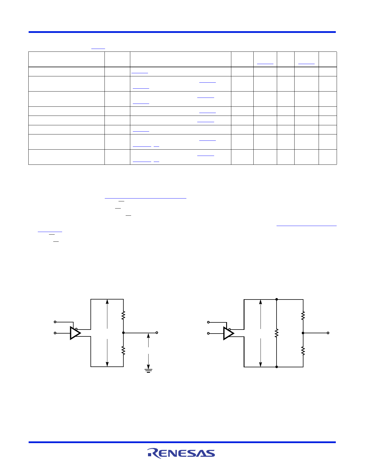
Test Circuits and Waveforms
VCC DE
DI
Z
D
Y
VOD
RL/2
RL/2 VOC
VCC DE
DI
Z
D
Y
VOD
375Ω
RL = 60Ω
VCM
-7V TO +12V
375Ω
FIGURE 4A. VOD AND VOC
FIGURE 4B. VOD WITH COMMON-MODE LOAD
FIGURE 4. DC DRIVER TEST CIRCUITS
FN6365 Rev. 6.00
Nov 9, 2017
Page 7 of 18
Share Link: