ISL3179E –ü—Ä–æ—Å–º–æ—Ç—Ä —Ç–µ—Ö–Ω–∏—á–µ—Å–∫–æ–≥–æ –æ–ø–∏—Å–∞–Ω–∏—è (PDF) - Renesas Electronics
–ù–æ–º–µ—Ä –≤ –∫–∞—Ç–∞–ª–æ–≥–µ
–ö–æ–º–ø–æ–Ω–µ–Ω—Ç—ã –û–ø–∏—Å–∞–Ω–∏–µ
–ø—Ä–æ–∏–∑–≤–æ–¥–∏—Ç–µ–ª—å
ISL3179E
Renesas Electronics

ISL3179E Datasheet PDF : 18 Pages
| |||
ISL3179E, ISL3180E
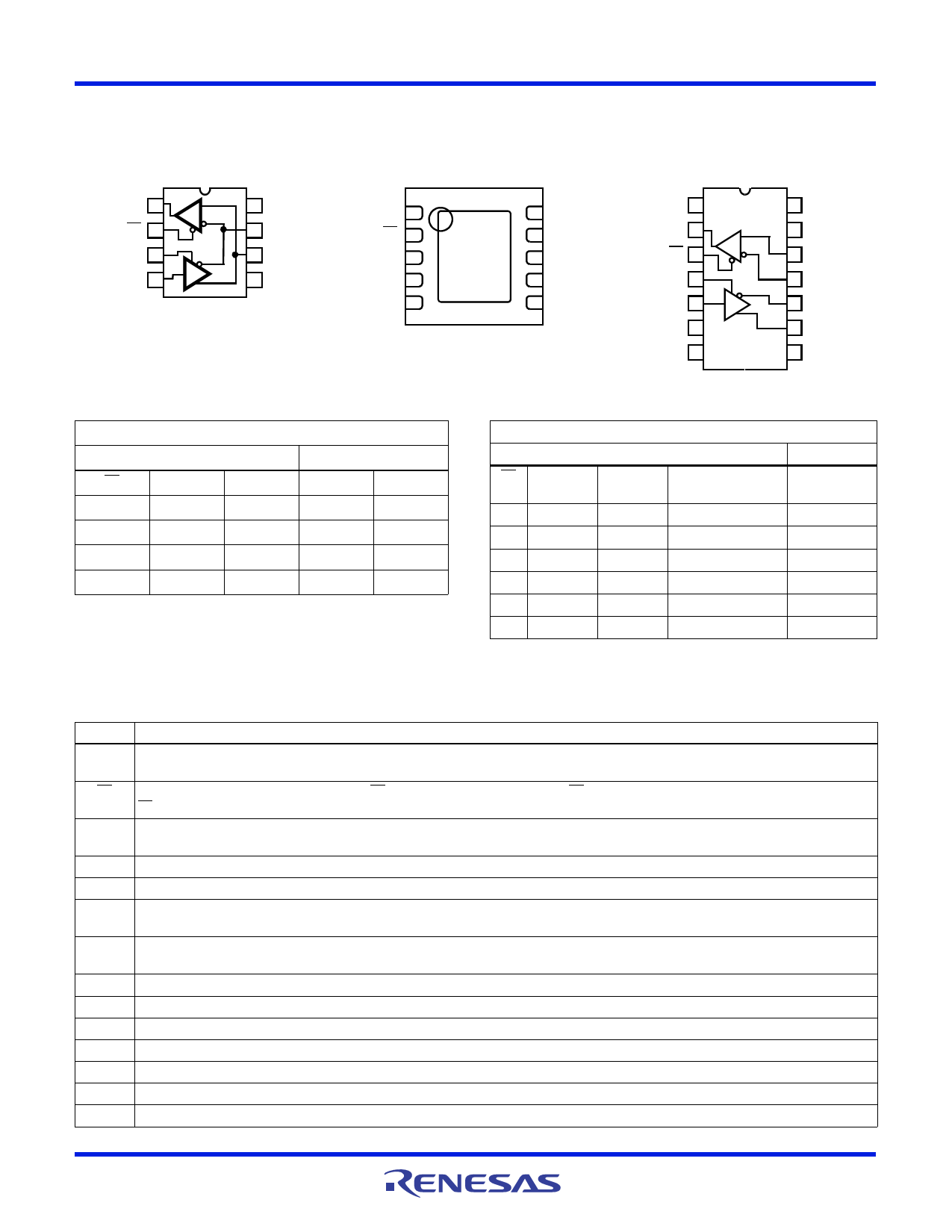
Pin Configurations
ISL3179E
(8 LD SOIC, MSOP)
TOP VIEW
RO 1
R
RE 2
DE 3
DI 4
D
8 VCC
7 B/Z
6 A/Y
5 GND
ISL3179E
(10 LD DFN)
TOP VIEW
RO 1
RE 2
DE 3
DI 4
NC 5
10 VCC
9 NC
EP
8 B/Z
7 A/Y
6 GND
ISL3180E
(14 LD SOIC)
TOP VIEW
NC 1
RO 2
RE 3
R
DE 4
DI 5
D
GND 6
GND 7
14 VCC
13 NC
12 A
11 B
10 Z
9Y
8 NC
Truth Table
TRANSMITTING
INPUTS
OUTPUTS
RE
DE
DI
B/Z
A/Y
X
1
1
0
1
X
1
0
1
0
0
0
X
High-Z
High-Z
1
0
X
High-Z*
High-Z*
NOTE: *Shutdown Mode
Truth Table
RECEIVING
INPUTS
OUTPUT
RE DE Half DE Full
A-B
RO
Duplex
Duplex
0
0
0
0
0
0
0
0
X
VAB ‚â• -0.05V
1
X
-0.05V > VAB > -0.2V Undetermined
X
VAB ≤ -0.2V
0
X
Inputs Open/Shorted
1
1
0
X
X
High-Z*
1
1
X
X
High-Z
NOTE: *Shutdown Mode
Pin Descriptions
PIN
FUNCTION
RO Receiver output: If A-B ≥ -50mV, RO is high; If A-B ≤ -200mV, RO is low; If A and B are unconnected (floating) or shorted, or connected to a
terminated bus that is undriven, RO is high.
RE Receiver output enable. RO is enabled when RE is low; RO is high impedance when RE is high. If the Rx enable function isn’t required, connect
RE directly to GND.
DE Driver output enable. The driver outputs, Y and Z, are enabled by bringing DE high, and they are high impedance when DE is low. If the Tx
enable function is not required, connect DE to VCC through a 1kΩ or greater resistor.
DI Driver input. A low on DI forces output Y low and output Z high. Similarly, a high on DI forces output Y high and output Z low.
GND Ground connection. This is also the potential of the DFN’s exposed metal pad.
A/Y ±16.5kV IEC61000 ESD protected RS-485/RS-422 level, noninverting receiver input and noninverting driver output. Pin is an input (A) if
DE = 0; pin is an output (Y) if DE = 1. ISL3179E only.
B/Z ±16.5kV IEC61000 ESD protected RS-485/RS-422 level, inverting receiver input and inverting driver output. Pin is an input (B) if DE = 0;
pin is an output (Z) if DE = 1. ISL3179E only.
A ±12kV HBM ESD protected RS-485/RS-422 level, noninverting receiver input. ISL3180E only.
B ±12kV HBM ESD protected RS-485/RS-422 level, inverting receiver input. ISL3180E only.
Y ±12kV HBM ESD protected RS-485/RS-422 level, noninverting driver output. ISL3180E only.
Z ±12kV HBM ESD protected RS-485/RS-422 level, inverting driver output. ISL3180E only.
VCC System power supply input (3.0V to 3.6V).
NC No internal connection.
EP The exposed metal pad on the bottom of the DFN; connect to GND.
FN6365 Rev. 6.00
Nov 9, 2017
Page 3 of 18
Share Link: