L5970AD Просмотр технического описания (PDF) - STMicroelectronics
Номер в каталоге
Компоненты Описание
производитель
L5970AD Datasheet PDF : 11 Pages
| |||
L5970AD
The turn on of the power element, or better, the rise time of the current at turn on, is a very critical param-
eter to compromise.
At a first approach, it looks like the faster it is the rise time, the lower are the turn on losses.
But there is a limit introduced by the recovery time of the recirculation diode.
In fact when the current of the power element equals the inductor current, the diode turns off and the drain
of the power is free to go high. But during its recovery time, the diode can be considered as an high value
capacitor and this produces a very high peak current, responsible of many problems:
Spikes on the device supply voltage that cause oscillations (and thus noise) due to the board parasitics.
Turn on overcurrent causing a decrease of the efficiency and system reliability.
Big EMI problems.
Shorter freewheeling diode life.
The fall time of the current during the turn off is also critical. In fact it produces voltage spikes (due to the
parasitics elements of the board) that increase the voltage drop across the PDMOS.
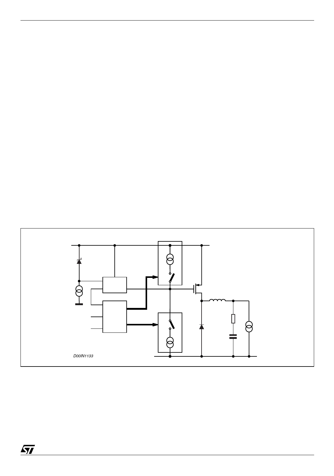
In order to minimize all these problems, a new topology of driving circuit has been used and its block dia-
gram is shown in fig. 8.
The basic idea is to change the current levels used to turn on and off the power switch, according with the
PDMOS status and with the gate clamp status.
This circuitry allow to turn off and on quickly the power switch and to manage the above question related
to the freewheeling diode recovery time problem. The gate clamp is necessary to avoid that Vgs of the
internal switch goes higher than Vgsmax. The ON/OFF Control block avoids any cross conduction be-
tween the supply line and ground.
Figure 8. Driving Circuitry
VCC
Vgsmax
CLAMP GATE
STOP
DRIVE
ON/OFF
CONTROL
DRAIN
OFF
ON
D00IN1133
IOFF
PDMOS
DRAIN
L
ESR
VOUT
ILOAD
C
ION
3.7 INHIBIT FUNCTION
The inhibit feature allows to put in stand-by mode the device. With INH pin higher than 2.2V the device is dis-
abled and the power consumption is reduced to less than 100µA. With INH pin lower than 0.8V, the device is
enabled. If the INH pin is left floating, an internal pull up ensures that the voltage at the pin reaches the inhibit
threshold and the device is disabled. The pin is also Vcc compatible.
7/11
Share Link: 