CAT93C56VP2I-T3 Просмотр технического описания (PDF) - Catalyst Semiconductor => Onsemi
Номер в каталоге
Компоненты Описание
производитель
CAT93C56VP2I-T3 Datasheet PDF : 18 Pages
| |||
CAT93C56, CAT93C57
Write
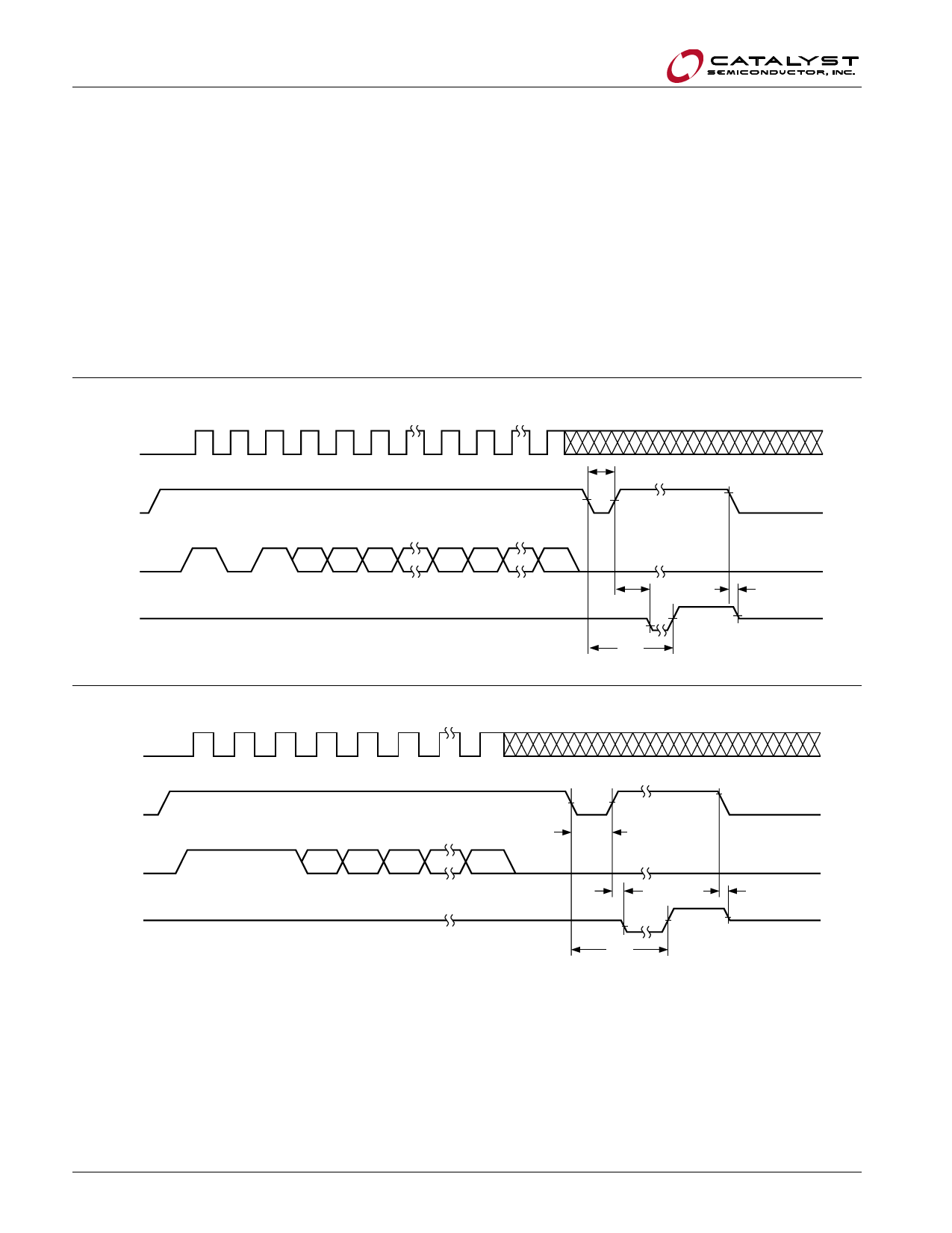
After receiving a WRITE command (Figure 4), address
and the data, the CS (Chip Select) pin must be
deselected for a minimum of tCSMIN. The falling edge of
CS will start the self clocking clear and data store cycle
of the memory location specified in the instruction. The
clocking of the SK pin is not necessary after the device
has entered the self clocking mode. The ready/busy
status of the CAT93C56/57 can be determined by
selecting the device and polling the DO pin. Since this
device features Auto-Clear before write, it is NOT
necessary to erase a memory location before it is
written into.
Erase
Upon receiving an ERASE command and address, the
CS (Chip Select) pin must be deasserted for a
minimum of tCSMIN (Figure 5). The falling edge of CS will
start the self clocking clear cycle of the selected
memory location. The clocking of the SaK pin is not
necessary after the device has entered the self clocking
mode. The ready/busy status of the CAT93C56/57 can
be determined by selecting the device and polling the
DO pin. Once cleared, the content of a cleared location
returns to a logical “1” state.
Figure 4. Write Instruction Timing
SK
CS
AN AN-1
DI
101
A0 DN
D0
tCSMIN
STATUS
VERIFY
STANDBY
tSV
BUSY
tHZ
HIGH-Z
DO
READY
HIGH-Z
tEW
Figure 5. Erase Instruction Timing
SK
CS
AN AN-1
A0
DI
1
1
1
STATUS VERIFY
tCS
STANDBY
tSV
tHZ
HIGH-Z
DO
BUSY READY
HIGH-Z
tEW
Doc. No. MD-1088 Rev. P
8
© Catalyst Semiconductor, Inc.
Characteristics subject to change without notice
Share Link: 