ZXM61P02F Просмотр технического описания (PDF) - ZP Semiconductor
Номер в каталоге
Компоненты Описание
производитель
ZXM61P02F Datasheet PDF : 3 Pages
| |||
ZXM61P02F
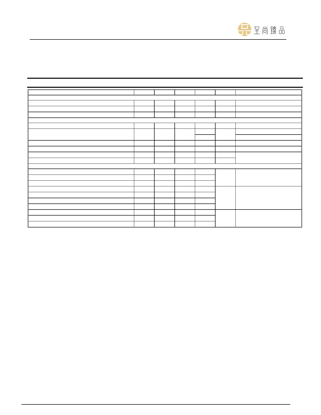
Electrical Characteristics @TA = 25°C unless otherwise specified
Characteristic
OFF CHARACTERISTICS
Drain-Source Breakdown Voltage
Zero Gate Voltage Drain Current
Gate-Source Leakage
ON CHARACTERISTICS
Gate Threshold Voltage
Symbol Min
Typ
BVDSS
-20
⎯
IDSS
⎯
⎯
IGSS
⎯
⎯
VGS(th)
-0.7
⎯
Static Drain-Source On-Resistance (Note 7)
RDS (ON)
⎯
⎯
Forward Transconductance (Notes 7 and 9)
Diode Forward Voltage (Note 7)
Reverse Recovery Time (Note 9)
Reverse Recovery Charge (Note 9)
DYNAMIC CHARACTERISTICS (Note 9)
Input Capacitance
Output Capacitance
Reverse Transfer Capacitance
Turn-On Delay Time (Note 8)
Turn-On Rise Time (Note 8)
Turn-Off Delay Time (Note 8)
Turn-Off Fall Time (Note 8)
Total Gate Charge (Note 8)
Gate-Source Charge (Note 8)
Gate-Drain Charge (Note 8)
gfs
VSD
trr
Qrr
Ciss
Coss
Crss
td(on)
tr
td(off)
tf
Qg
Qgs
Qgd
0.56
⎯
⎯
⎯
⎯
⎯
⎯
⎯
⎯
⎯
⎯
⎯
⎯
⎯
⎯
⎯
14.9
5.6
150
70
30
2.9
6.7
11.2
10.1
3.5
0.5
1.5
Notes:
7. Measured under pulsed conditions. Pulse width = 300μs. Duty cycle ≤ 2%.
8. Switching characteristics are independent of operating junction temperature.
9. For design aid only, not subject to production testing.
Max
⎯
-0.1
±100
⎯
0.6
0.9
⎯
-0.95
⎯
⎯
⎯
⎯
⎯
⎯
⎯
⎯
⎯
⎯
⎯
⎯
Unit
Test Condition
V ID = -250μA, VGS = 0V
μA VDS = -20V, VGS = 0V
nA VGS = ±12V, VDS = 0V
V
ID = -250μA, VDS = VGS
Ω
VGS = -4.5V, ID = -0.61A
VGS = -2.7V, ID = -0.31A
S VDS = -10V, ID = -0.31A
V TJ = 25°C, IS = -0.61A, VGS = 0V
ns TJ = 25°C, IF = -0.61A,
nC di/dt = 100A/μs
pF VDS = -15V, VGS = 0V
f = 1.0MHz
ns
VDD = -110V, ID = -0.93A,
RG ≅ 6.2Ω, RD ≅ 11Ω,
nC VDS = -16V, VGS = -4.5V,
ID = -0.61A
sales@zpsemi.com
www.zpsemi.com
3 of 3
Share Link: 