UPC2708TB Просмотр технического описания (PDF) - California Eastern Laboratories.
Номер в каталоге
Компоненты Описание
производитель
UPC2708TB Datasheet PDF : 8 Pages
| |||
UPC2708TB
PIN DESCRIPTIONS
Pin No.
1
Symbol
Input
Applied
Pin
Voltage (V) Voltage (V)
–
1.16
4
Output
–
6
VCC
4.5 to 5.5
–
2
GND
0
–
3
5
Description
Signal input pin. An internal matching circuit,
configured with resistors, enables 50 Ω connection
over a wide bandwidth. A multi-feedback circuit is
designed to cancel the deviations of hFE and
resistance. This pin must be coupled to the signal
source with a blocking capacitor.
Signal output pin. Connect an inductor between
this pin and VCC to supply current to the internal
output transistors.
Power supply pin. This pin should be externally
equipped with a bypass capacitor to minimize
ground impedance.
Ground pins. These pins should be connected to
system ground with minimum inductance. Ground
pattern on the board should be formed as wide as
possible. All the ground pins must be connected
together with wide ground pattern to minimize
impedance difference.
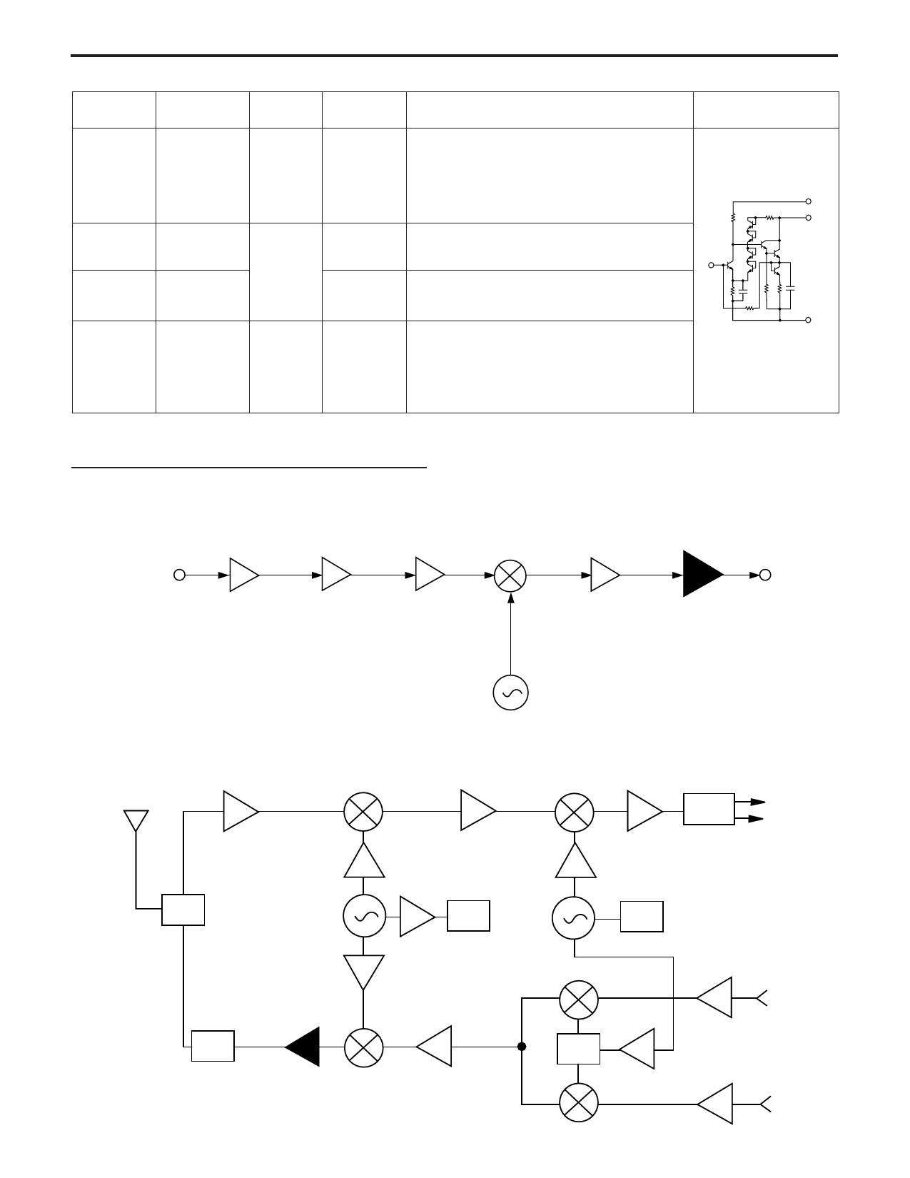
Internal Equivalent
Circuit
6
VCC
OUT
4
1
IN
2, 3, 5
SYSTEM APPLICATION EXAMPLE
EXAMPLE OF DBS CONVERTERS
Parabola
Antenna
BS Antenna
(DBS ODU)
RF Amp.
Mixer
UPC2711TB
UPC2712TB
IF Amp.
To
IDU
UPC2708TB
EXAMPLE OF 2.4 GHz BAND RECEIVER
RX
Oscillator
DEMO
I
Q
SW
PLL
PLL
TX PA
Driver
UPC2708TB
I
0˚
φ
90˚
Q
Share Link: 