FXL4TD245 Просмотр технического описания (PDF) - ON Semiconductor
Номер в каталоге
Компоненты Описание
производитель
FXL4TD245 Datasheet PDF : 16 Pages
| |||
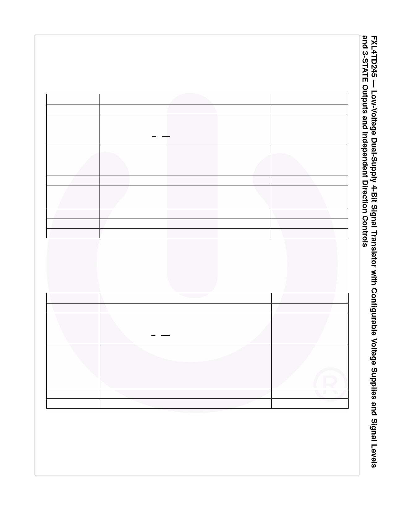
Absolute Maximum Ratings
The “Absolute Maximum Ratings” are those values beyond which the safety of the device cannot be guaranteed.
The device should not be operated at these limits. The parametric values defined in the Electrical Characteristics
tables are not guaranteed at the absolute maximum ratings. The “Recommended Operating Conditions” table will
define the conditions for actual device operation.
Symbol
Parameter
Rating
VCCA, VCCB
VI
VO
IIK
IOK
IOH / IOL
ICC
TSTG
Supply Voltage
DC Input Voltage
I/O Port A
I/O Port B
Control Inputs (T/Rn, OE)
Output Voltage(1)
Outputs 3-STATE
Outputs Active (An)
Outputs Active (Bn)
DC Input Diode Current @ VI < 0V
DC Output Diode Current @
VO < 0V
VO > VCC
DC Output Source/Sink Current
DC VCC or Ground Current per Supply Pin
Storage Temperature Range
−0.5V to +4.6V
−0.5V to +4.6V
−0.5V to +4.6V
−0.5V to +4.6V
−0.5V to +4.6V
−0.5V to VCCA + 0.5V
−0.5V to VCCB + 0.5V
−50mA
−50mA
+50mA
−50mA / +50mA
±100mA
−65°C to +150°C
Recommended Operating Conditions(2)
The Recommended Operating Conditions table defines the conditions for actual device operation. Recommended
operating conditions are specified to ensure optimal performance to the datasheet specifications. Fairchild does not
recommend exceeding them or designing to Absolute Maximum Ratings.
Symbol
VCCA or VCCB
TA
Δt /ΔV
Parameter
Power Supply Operating
Input Voltage
Port A
Port B
Control Inputs (T/Rn, OE)
Output Current in IOH/IOL with VCC @
3.0V to 3.6V
2.3V to 2.7V
1.65V to 1.95V
1.4V to 1.65V
1.1V to 1.4V
Free Air Operating Temperature
Maximum Input Edge Rate VCCA/B = 1.1V to 3.6V
Rating
1.1V to 3.6V
0.0V to 3.6V
0.0V to 3.6V
0.0V to VCCA
±24mA
±18mA
±6mA
±2mA
±0.5mA
−40°C to +85°C
10ns/V
Notes:
1. IO Absolute Maximum Rating must be observed.
2. All unused inputs and I/O pins must be held at VCCI or GND.
©2006 Fairchild Semiconductor Corporation
FXL4TD245 • Rev. 1.0.6
4
www.fairchildsemi.com
Share Link: 