FXL4TD245 Просмотр технического описания (PDF) - ON Semiconductor
Номер в каталоге
Компоненты Описание
производитель
FXL4TD245 Datasheet PDF : 16 Pages
| |||
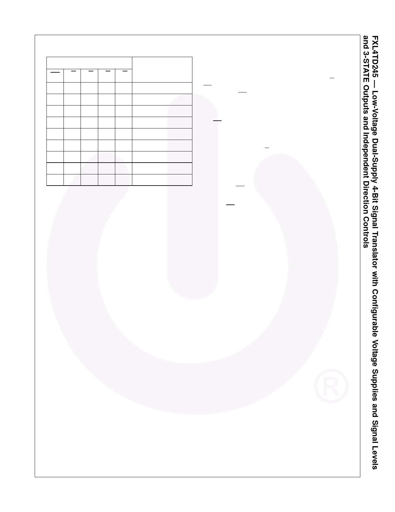
Truth Table
Inputs
OE T/R0 T/R1 T/R2 T/R3
Outputs
L L X X X B0 Data to A0 Output
L H X X X A0 Data to B0 Output
L X L X X B1 Data to A1 Output
L X H X X A1 Data to B1 Output
L X X L X B2 Data to A2 Output
L X X H X A2 Data to B2 Output
L X X X L B3 Data to A3 Output
L X X X H A3 Data to B3 Output
H X X X X 3-State
H = HIGH Voltage Level
L = LOW Voltage Level
X = Don't Care
Power-Up/Power-Down Sequencing
FXL translators offer an advantage in that either VCC
may be powered up first. This benefit derives from the
chip design. When either VCC is at 0 volts, outputs are in
a HIGH-Impedance state. The control inputs (T/Rn and
OE) are designed to track the VCCA supply. A pull-up
resistor tying OE to VCCA should be used to ensure that
bus contention, excessive currents, or oscillations do not
occur during power-up/power-down. The size of the pull-
up resistor is based upon the current-sinking capability of
the OE driver.
The recommended power-up sequence is the following:
1. Apply power to either VCC.
2. Apply power to the T/Rn inputs (Logic HIGH for A-to-B
operation; Logic LOW for B-to-A operation) and to the
respective data inputs (A Port or B Port). This may
occur at the same time as Step 1.
3. Apply power to other VCC.
4. Drive the OE input LOW to enable the device.
The recommended power-down sequence is the following:
1. Drive OE input HIGH to disable the device.
2. Remove power from either VCC.
3. Remove power from other VCC.
©2006 Fairchild Semiconductor Corporation
FXL4TD245 • Rev. 1.0.6
3
www.fairchildsemi.com
Share Link: 