HIN207ECAZ Просмотр технического описания (PDF) - Renesas Electronics
Номер в каталоге
Компоненты Описание
производитель
HIN207ECAZ
Renesas Electronics

HIN207ECAZ Datasheet PDF : 20 Pages
| |||
HIN202, HIN206, HIN207, HIN208, HIN211, HIN213
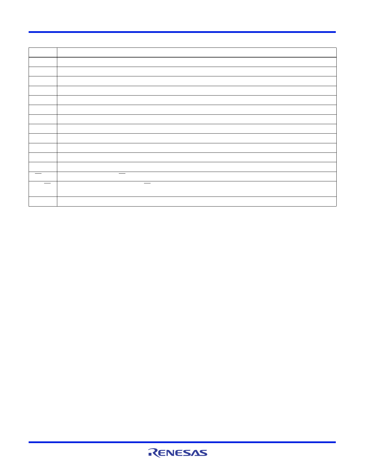
Pin Descriptions
PIN
FUNCTION
VCC
V+
Power Supply Input 5V 10%, (5V 5% HIN207).
Internally generated positive supply (+10V nominal).
V-
Internally generated negative supply (-10V nominal).
GND Ground Lead. Connect to 0V.
C1+ External capacitor (+ terminal) is connected to this lead.
C1- External capacitor (- terminal) is connected to this lead.
C2+ External capacitor (+ terminal) is connected to this lead.
C2- External capacitor (- terminal) is connected to this lead.
TIN
TOUT
RIN
ROUT
EN, EN
Transmitter Inputs. These leads accept TTL/CMOS levels. An internal 400kpull-up resistor to VCC is connected to each lead.
Transmitter Outputs. These are RS-232 levels (nominally 10V).
Receiver Inputs. These inputs accept RS-232 input levels. An internal 5kpull-down resistor to GND is connected to each input.
Receiver Outputs. These are TTL/CMOS levels.
Receiver enable Input. With EN = 5V (HIN213 EN = 0V), the receiver outputs are placed in a high impedance state.
SD, SD Shutdown Input. With SD = 5V (HIN213 SD = 0V), the charge pump is disabled, the receiver outputs are in a high impedance state
(except R4 and R5 of HIN213) and the transmitters are shut off.
NC
No Connect. No connections are made to these leads.
FN3980 Rev 19.00
August 6, 2015
Page 3 of 20
Share Link: