HI5828 Просмотр технического описания (PDF) - Renesas Electronics
Номер в каталоге
Компоненты Описание
производитель
HI5828 Datasheet PDF : 12 Pages
| |||
HI5828
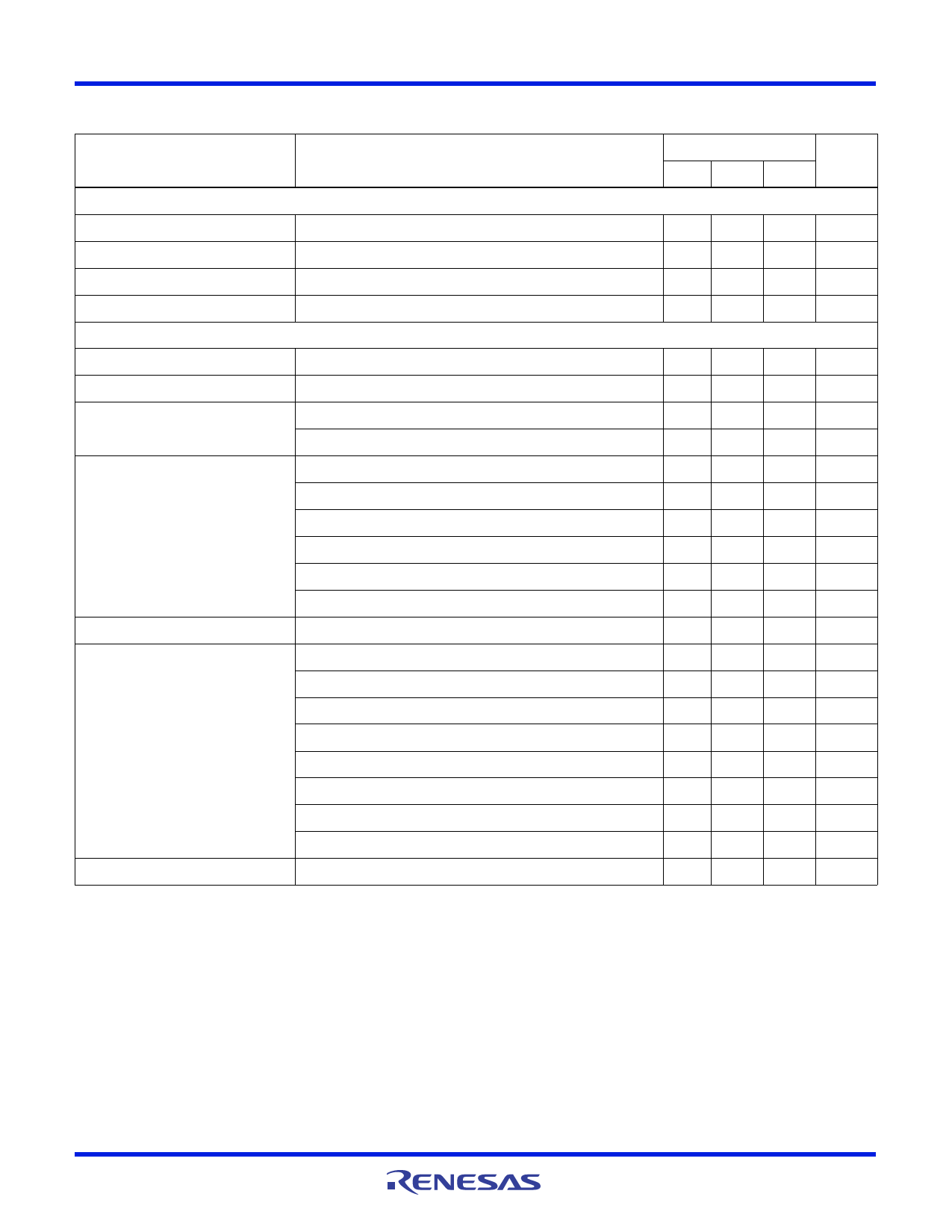
Electrical Specifications
PARAMETER
AVDD = DVDD = +5V
IOUTFS = 20mA, TA
(except
= 25oC
where otherwise noted), VREF = Internal
for All Typical Values (Continued)
1.2V,
TA = -40oC TO 85oC
TEST CONDITIONS
MIN TYP MAX
UNITS
TIMING CHARACTERISTICS
Data Setup Time, tSU
See Figure 4 (Note 3)
Data Hold Time, tHLD
See Figure 4 (Note 3)
Propagation Delay Time, tPD
See Figure 4
CLK Pulse Width, tPW1, tPW2
See Figure 4 (Note 3)
POWER SUPPLY CHARACTERISTICS
-
1.5
-
ns
-
1.2
-
ns
-
2.5
-
ns
4
-
-
ns
AVDD Power Supply
DVDD Power Supply
Analog Supply Current (IAVDD)
(Note 9)
(Note 9)
5V or 3V, IOUTFS = 20mA (Note 7)
5V or 3V, IOUTFS = 2mA
2.7
5.0
5.5
V
2.7
5.0
5.5
V
-
44
50
mA
-
7
-
mA
Digital Supply Current (IDVDD)
5V (Note 5)
5V (Note 6)
-
12
-
mA
-
17.6
-
mA
5V (Note 7)
-
29
38
mA
3V (Note 5)
-
4
-
mA
3V (Note 6)
-
8.2
-
mA
3V (Note 7)
-
9.6
12
mA
Supply Current (IAVDD) Sleep Mode
Power Dissipation
5V or 3V, IOUTFS = Don’t Care
5V, IOUTFS = 20mA (Note 5)
-
2.7
-
mA
-
280
-
mW
5V, IOUTFS = 20mA (Note 6)
-
312
-
mW
5V, IOUTFS = 20mA (Note 7)
-
365
440
mW
5V, IOUTFS = 2mA (Note 6)
-
137
-
mW
3V, IOUTFS = 20mA (Note 5)
-
144
-
mW
3V, IOUTFS = 20mA (Note 6)
-
158
mW
3V, IOUTFS = 20mA (Note 7)
-
161
177
mW
3V, IOUTFS = 2mA (Note 6)
-
46
-
mW
Power Supply Rejection
Single Supply (Note 8)
-0.2
-
+0.2 % FSR/V
NOTES:
2. Gain Error measured as the error in the ratio between the full scale output current and the current through RSET (typically 625A). Ideally the
ratio should be 32.
3. Parameter guaranteed by design or characterization and not production tested.
4. Spectral measurements made with differential transformer coupled output and no external filtering.
5. Measured with the clock at 60MSPS and the output frequency at 10MHz.
6. Measured with the clock at 100MSPS and the output frequency at 40MHz.
7. Measured with the clock at 130MSPS and the output frequency at 5MHz.
8. See “Definition of Specifications”.
9. It is recommended that the output current be reduced to 12mA or less to maintain optimum performance for operation below 3V. DVDD and AVDD
do not have to be equal.
FN4658 Rev 3.00
April 2001
Page 8 of 12
Share Link: 