HI5828 Просмотр технического описания (PDF) - Renesas Electronics
Номер в каталоге
Компоненты Описание
производитель
HI5828 Datasheet PDF : 12 Pages
| |||
HI5828
Absolute Maximum Ratings
Digital Supply Voltage DVDD to DGND . . . . . . . . . . . . . . . . . . +5.5V
Analog Supply Voltage AVDD to AGND . . . . . . . . . . . . . . . . . . +5.5V
Grounds, AGND TO DGND . . . . . . . . . . . . . . . . . . . . -0.3V to +0.3V
Digital Input Voltages (D11-D0, CLK, SLEEP) . . . . . . . DVDD + 0.3V
Reference Input Voltage Range. . . . . . . . . . . . . . . . . . .AVDD + 0.3V
Analog Output Current (IOUTA/B, QOUTA/B) . . . . . . . . . . . . . 24mA
Operating Conditions
Temperature Range . . . . . . . . . . . . . . . . . . . . . . . . . . -40oC to 85oC
Thermal Information
Thermal Resistance (Typical, Note 1)
JA(oC/W)
LQFP Package. . . . . . . . . . . . . . . . . . . . . . . . . . . . .
70
Maximum Junction Temperature . . . . . . . . . . . . . . . . . . . . . . .150oC
Maximum Storage Temperature Range . . . . . . . . . . -65oC to 150oC
Maximum Lead Temperature (Soldering 10s) . . . . . . . . . . . . .300oC
(LQFP - Lead Tips Only)
CAUTION: Stresses above those listed in “Absolute Maximum Ratings” may cause permanent damage to the device. This is a stress only rating and operation of the
device at these or any other conditions above those indicated in the operational sections of this specification is not implied.
NOTE:
1. JA is measured with the component mounted on a low effective thermal conductivity test board in free air. See Tech Brief TB379 for details.
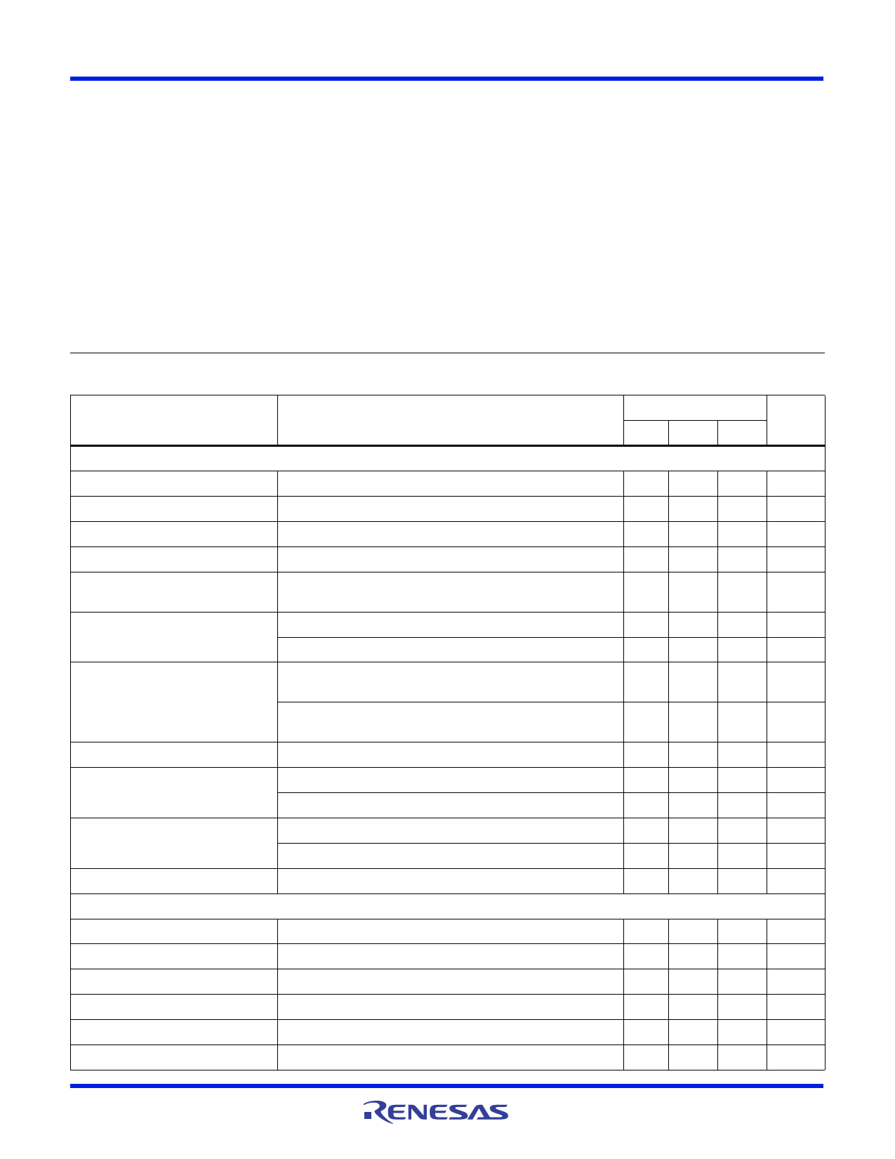
Electrical Specifications
PARAMETER
AVDD = DVDD = +5V
IOUTFS = 20mA, TA
(except
= 25oC
where otherwise noted),
for All Typical Values
VREF
=
Internal
1.2V,
TA = -40oC TO 85oC
TEST CONDITIONS
MIN TYP MAX
UNITS
SYSTEM PERFORMANCE
Resolution
12
-
-
Bits
Integral Linearity Error, INL
“Best Fit” Straight Line (Note 8)
-2.0 0.75 +2.0
LSB
Differential Linearity Error, DNL
(Note 8)
-1.0 0.5 +1.0
LSB
Offset Error, IOS
Offset Drift Coefficient
(Note 8)
(Note 8)
-0.025
-
+0.025 % FSR
-
0.1
-
ppm
FSR/oC
Full Scale Gain Error, FSE
With External Reference (Notes 2, 8)
-10
2
+10 % FSR
With Internal Reference (Notes 2, 8)
-10
1
+10 % FSR
Full Scale Gain Drift
With External Reference (Note 8)
-
50
-
ppm
FSR/oC
With Internal Reference (Note 8)
-
100
-
ppm
FSR/oC
Full Scale Output Current, IFS
Crosstalk
Gain Matching Between Channels
(DC Measurement)
fCLK = 100MSPS, fOUT = 10MHz
fCLK = 100MSPS, fOUT = 40MHz
As a percentage of Full Scale Range
In dB Full Scale Range
2
-
20
mA
-
85
-
dB
-
64
-
dB
-5
-
+5 % FSR
-0.445
-
+0.420 dB FSR
Output Voltage Compliance Range (Note 3, 8)
-0.3
-
1.25
V
DYNAMIC CHARACTERISTICS
Maximum Clock Rate, fCLK
Output Settling Time, (tSETT)
Singlet Glitch Area (Peak Glitch)
Output Rise Time
(Note 3)
0.05% (2 LSB) (Note 8)
RL = 25(Note 8)
Full Scale Step
130
-
-
MHz
-
35
-
ns
-
5
-
pV•s
-
2.5
-
ns
Output Fall Time
Full Scale Step
-
2.5
-
ns
Output Capacitance
-
10
-
pF
FN4658 Rev 3.00
April 2001
Page 5 of 12
Share Link: 