HI5828 Просмотр технического описания (PDF) - Renesas Electronics
Номер в каталоге
Компоненты Описание
производитель
HI5828 Datasheet PDF : 12 Pages
| |||
HI5828
Ground Planes
Separate digital and analog ground planes should be used. All
of the digital functions of the device and their corresponding
components should be located over the digital ground plane
and terminated to the digital ground plane. The same is true for
the analog components and the analog ground plane. Consult
Application Note AN9855.
Noise Reduction
To minimize power supply noise, 0.1F capacitors should be
placed as close as possible to the converter’s power supply
pins, AVDD and DVDD. Also, the layout should be designed
using separate digital and analog ground planes and these
capacitors should be terminated to the digital ground for DVDD
and to the analog ground for AVDD. Additional filtering of the
power supplies on the board is recommended.
Voltage Reference
The internal voltage reference of the device has a nominal value
of + 1.2V with a 10ppm/oC drift coefficient over the full
temperature range of the converter. It is recommended that a
0.1F capacitor be placed as close as possible to the REFIO
pin, connected to the analog ground. The REFLO pin (18)
selects the reference. The internal reference can be selected if
pin 18 is tied low (ground). If an external reference is desired,
then pin 18 should be tied high (the analog supply voltage) and
the external reference driven into REFIO, pin 17. The full scale
output current of the converter is a function of the voltage
reference used and the value of RSET. IOUT should be within
the 2mA to 20mA range, though operation below 2mA is
possible, with performance degradation.
VFSADJ and VREFIO will be equivalent except for a small offset
voltage. If the internal reference is used, VFSADJ will equal
approximately 1.2V on the FSADJ pin (20). If an external
reference is used, VFSADJ will equal the external reference.
The calculation for IOUT(Full Scale) is:
IOUT(Full Scale) = (VFSADJ/RSET) X 32.
If the full scale output current is set to 20mA by using the
internal voltage reference (1.2V) and a 1.91k RSET resistor,
then the input coding to output current will resemble the
following:
TABLE 1. INPUT CODING vs OUTPUT CURRENT
INPUT CODE (D11-D0) I/QOUTA (mA)
I/QOUTB (mA)
11 11111 11111
20
0
10 00000 00000
10
10
00 00000 00000
0
20
Outputs
The 5 MSBs for each DAC on the HI5828 drive a thermometer
decoder, which is a digital decoder that has an N-bit (5 bits for
the HI5828) binary coded input word with 2N-1 (31 for the
HI5828) output bits, where the number of output bits that are
active correlate directly to the input binary word. The HI5828
uses a thermometer decoder to significantly minimize the
output glitch energy for each DAC. I/QOUTA and I/QOUTB are
complementary current outputs. The sum of the two currents is
always equal to the full scale output current minus one LSB. If
single ended use is desired, a load resistor can be used to
convert the output current to a voltage. It is recommended that
the unused output be either grounded or equally terminated.
The voltage developed at the output must not violate the output
voltage compliance range of -0.3V to 1.25V. RLOAD (the
impedance loading each current output) should be chosen so
that the desired output voltage is produced in conjunction with
the output full scale current. If a known line impedance is to be
driven, then the output load resistor should be chosen to match
this impedance. The output voltage equation is:
VOUT = IOUT X RLOAD.
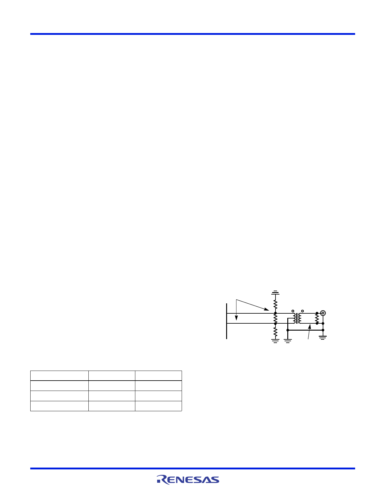
These outputs can be used in a differential-to-single-ended
arrangement to achieve better harmonic rejection. The SFDR
measurements in this data sheet were performed with a 1:1
transformer on the output of the DAC (see Figure 1). With the
center tap grounded, the output swing of pins 15/22 and 16/21
will be biased at zero volts. The loading as shown in Figure 1
will result in a 500mV signal at the output of the transformer if
the full scale output current of the DAC is set to 20mA. VOUT =
2 x IOUT x REQ, where REQ is ~12.5.
REQ IS THE IMPEDANCE
LOADING EACH OUTPUT.
PIN 15/22
PIN 16/21
HI5828
50
I/QOUTA
100
I/QOUTB
50
VOUT = (2 x IOUT x REQ)V
50
50REPRESENTS THE
SPECTRUM ANALYZER
FIGURE 1.
Allowing the center tap to float will result in identical
transformer output, however the output pins of the DAC will
have positive DC offset. Since the DAC’s output voltage
compliance range is -0.3V to +1.25V, the center tap may need
to be left floating or DC offset in order to increase the amount
of signal swing available. The 50 load on the output of the
transformer represents the spectrum analyzer’s input
impedance.
FN4658 Rev 3.00
April 2001
Page 10 of 12
Share Link: 