HCPL-8100 Просмотр технического описания (PDF) - Avago Technologies
Номер в каталоге
Компоненты Описание
производитель
HCPL-8100 Datasheet PDF : 10 Pages
| |||
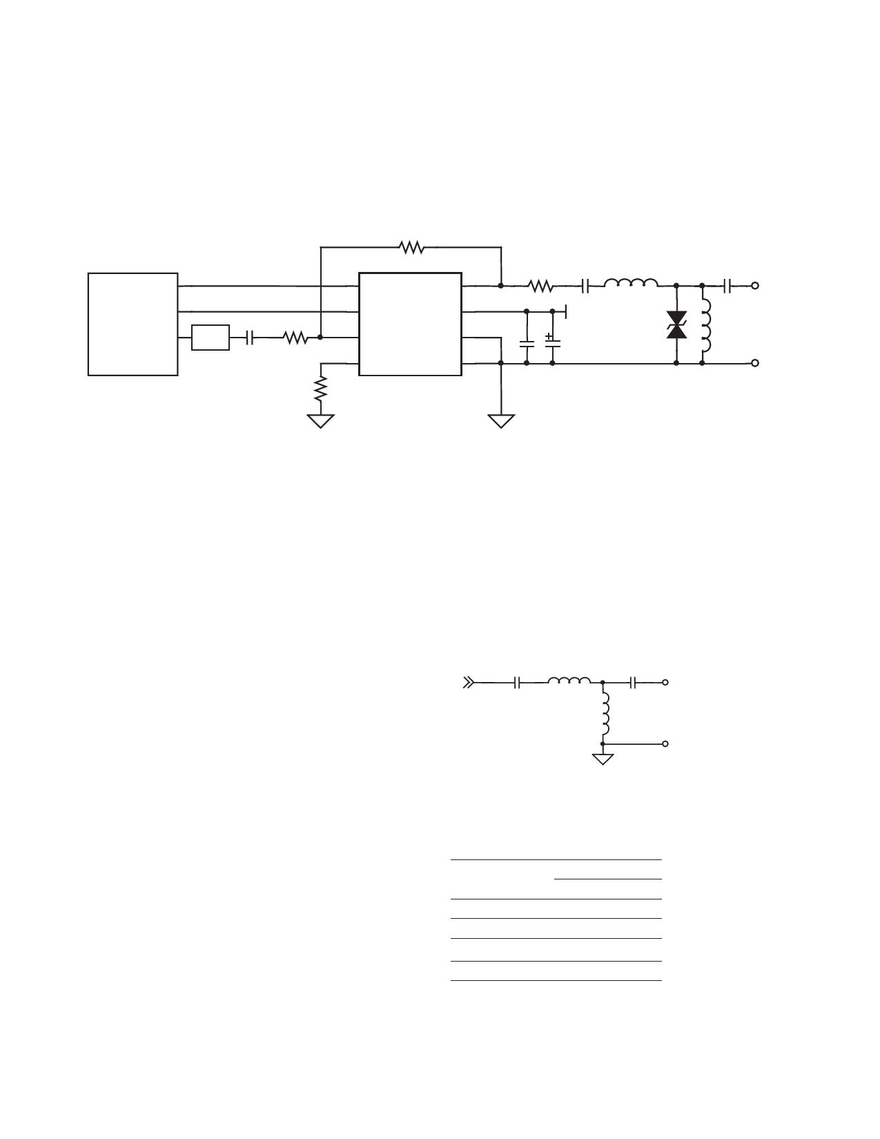
Application Information
The HCPL-8100 and HCPL-0810 are designed to work with
various transceivers and can be used with a variety of
modulation methods including ASK, FSK and BPSK. Figure
17 shows a typical application in a powerline modem using
Frequency Shift Keying (FSK) modulation scheme.
R2
Gain = − R2 / R1
STATUS
TX-EN
TX
PLM
Transceiver
F ilter
C1 R1
100 nF
Rref
24 kΩ
1
Status
2
Tx-en
3
Tx-in
8
Tx -out
7
VCC
6
GND
4
R ref
5
GND
HCPL - 8100/0810
Figure 17. Schematic of HCPL-8100 or HCPL-0810 application for FSK modulation scheme.
R3
C3
2 Ω 1 µF
L2
5V
C5
C4 100 µF
100 nF
C2
L
D1 X2
L1
330 µH
N
Line Driver
The line driver is capable of driving powerline load imped-
ances with output signals up to 4 VPP. The internal biasing
of the line driver is controlled externally via a resistor Rref
connected from pin 4 to ground. The optimum biasing
point value for modulation frequencies up to 150 kHz
is 24 kΩ. For higher frequency operation with certain
modulation schemes, it may be necessary to reduce the
resistor value to enable compliance with international
regulations.
The output of the line driver is coupled onto the powerline
using a simple LC coupling circuit as shown in Figure
18. Refer to Table 1 for some typical component values.
Capacitor C2 and inductor L1 attenuate the 50/60 Hz
powerline transmission frequency. A suitable value for
L1 can range in value from 200 µH to 1 mH. To reduce the
series coupling impedance at the modulation frequency,
L2 is included to compensate the reactive impedance of
C2. This inductor should be a low resistive type capable
of meeting the peak current requirements. To meet many
regulatory requirements, capacitor C2 needs to be an X2
type. Since these types of capacitors typically have a very
wide tolerance range of 20%, it is recommended to use as
low Q factor as possible for the L2/C2 combination. Using
a high Q coupling circuit will result in a wide tolerance on
the overall coupling impedance, causing potential commu-
nication difficulties with low powerline impedances. Occa-
sionally with other circuit configurations, a high Q coupling
arrangement is recommended, e.g., C2 less than 100 nF. In
this case it is normally used as a compromise to filter out
of band harmonics originating from the line driver. This is
not required with the HCPL-8100 or HCPL-0810.
C3
L2
Tx
1 µF
C2
L
X2
L1
N
GND
Figure 18. LC coupling network.
Table 1. Typical component values
for LC coupling network.
Carrier
Frequency (kHz)
110
LC Coupling
L2 (µH) C2 (nF)
15 150
120
10 220
132
6.8 220
150
6.8 220
Share Link: 