CAT24C21WE-T3 Просмотр технического описания (PDF) - ON Semiconductor
Номер в каталоге
Компоненты Описание
производитель
CAT24C21WE-T3 Datasheet PDF : 14 Pages
| |||
CAT24C21
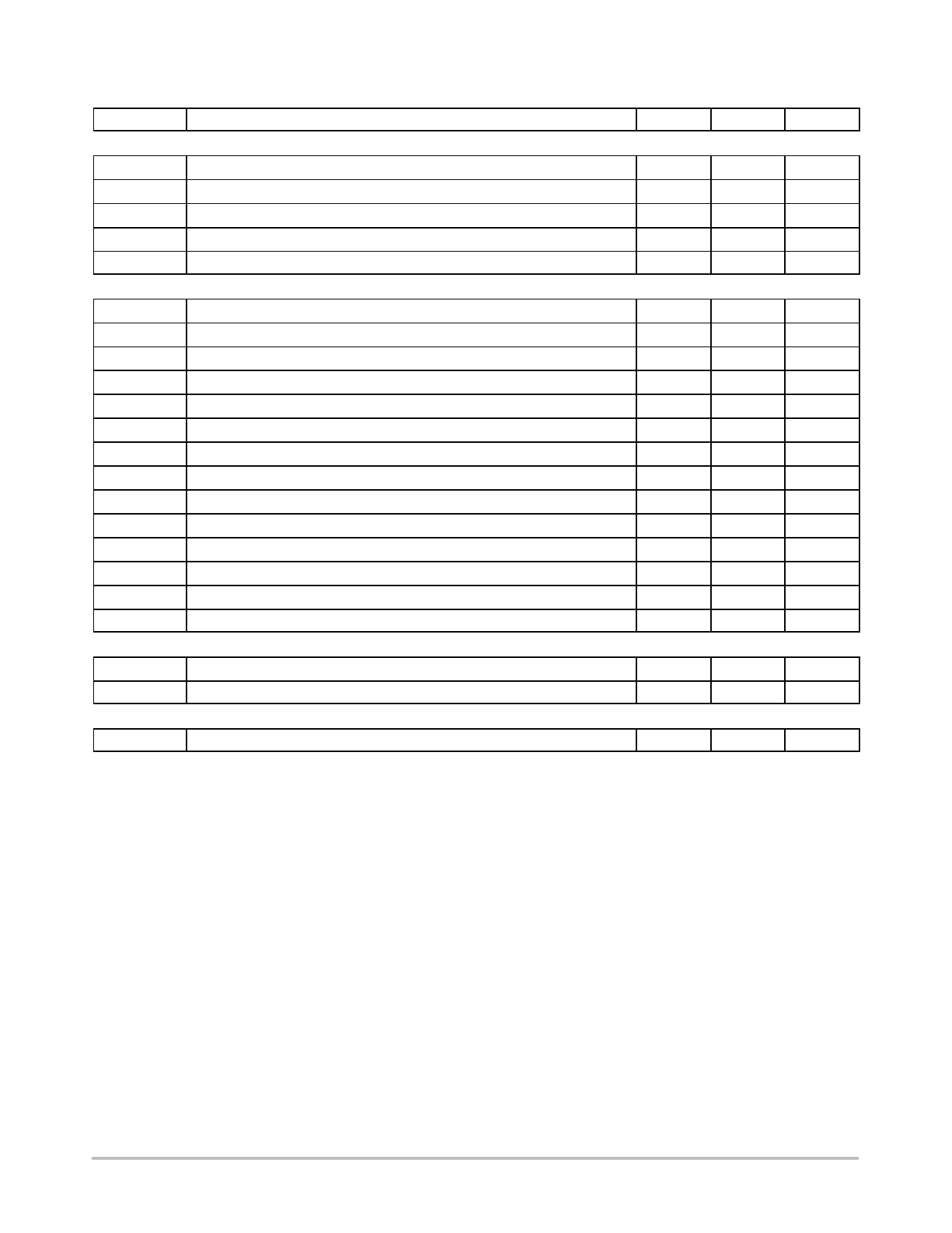
Table 5. A.C. CHARACTERISTICS (VCC = 2.5 V to 5.5 V, unless otherwise specified. Industrial temperature range.)
Symbol
Parameter
Min
Max
TRANSMIT−ONLY MODE
TVAA
Output valid from VCLK
TVHIGH
VCLK high
TVLOW
VCLK low
TVHZ
Mode transition
TVPU
Transmit−only power−up
READ & WRITE CYCLE LIMITS
0.5
0.6
1.3
0.5
0
FSCL
Clock Frequency
TI (Note 8) Noise Suppression Time Constant at SCL, SDA Inputs
tAA
SCL Low to SDA Data Out and ACK Out
tBUF (Note 8) Time the Bus Must be Free Before a New Transmission Can Start
tHD:STA
Start Condition Hold Time
tLOW
Clock Low Period
tHIGH
Clock High Period
tSU:STA
Start Condition Setup Time
tHD:DAT
Data In Hold Time
tSU:DAT
Data In Setup Time
tR (Note 8) SDA and SCL Rise Time
tF (Note 8) SDA and SCL Fall Time
tSU:STO
Stop Condition Setup Time
tDH
Data Out Hold Time
POWER−UP TIMING (Note 8 and 9)
400
100
1
1.2
0.6
1.2
0.6
0.6
0
50
0.3
300
0.6
100
tPUR
Power−up to Read Operation
1
tPUW
Power−up to Write Operation
1
WRITE CYCLE LIMITS
tWR
Write Cycle Time
5
8. This parameter is tested initially and after a design or process change that affects the parameter.
9. tPUR and tPUW are the delays required from the time VCC is stable until the specified operation can be initiated.
Units
ms
ms
ms
ms
ns
kHz
ns
ms
ms
ms
ms
ms
ms
ns
ns
ms
ns
ms
ns
ms
ms
ms
The write cycle time is the time from a valid stop condition
of a write sequence to the end of the internal program/erase
cycle. During the write cycle, the bus interface circuits are
disabled, SDA is allowed to remain high, and the device
does not respond to its slave address.
Pin Description
The SCL serial clock input pin is used to clock all data
transfers into or out of the device when in the bi−directional
mode.
The SDA bi−directional serial data/address pin is used to
transfer data into and out of the device. The SDA pin is an
open drain output and can be wire−ORed with other open
drain or open collector outputs.
Functional Description
The CAT24C21 has two modes of operation: the
transmit−only mode and the bi−directional mode. There is a
separate 2−wire protocol to support each mode, each having
a separate clock input (VCLK and SCL respectively) and
both modes sharing a common bi−directional data line
(SDA). The CAT24C21 enters the transmit−only mode upon
power up and begins outputting data on the SDA pin with
each clock signal on the VCLK pin. The device will remain
in the transmit−only mode until there is a valid HIGH to
LOW transition on the SCL pin, when it will switch to the
bi−directional mode (Figure 2). Once in the bi−directional
mode, the only way to return to the transmit−only mode is
by powering down the device.
The VCLK serial clock input pin is used to clock data out
of the device when in transmit−only mode. When held low,
in bi−directional mode, it will inhibit write operations.
http://onsemi.com
3
Share Link: 