TS613IDW Просмотр технического описания (PDF) - STMicroelectronics
Номер в каталоге
Компоненты Описание
производитель
TS613IDW Datasheet PDF : 10 Pages
| |||
TS613
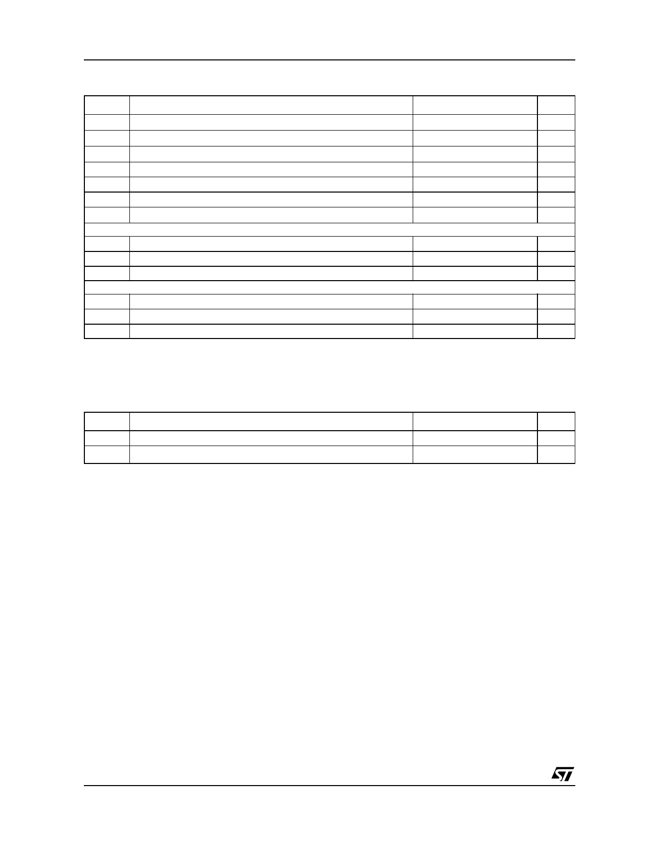
ABSOLUTE MAXIMUM RATINGS
Symbol
Parameter
Value
VCC
Vid
Vin
Toper
Tstd
Tj
Supply voltage 1)
Differential Input Voltage 2)
Input Voltage Range 3)
Operating Free Air Temperature Range
Storage Temperature
Maximum Junction Temperature
Output Short Circuit Duration
±7
±2
±6
-40 to + 85
-65 to +150
150
4)
SO8
Rthjc Thermal Resistance Junction to Case
28
Rthja Thermal Resistance Junction to Ambient Area
175
Pmax. Maximum Power Dissipation (@25°C)
715
SO8 Exposed-Pad
Rthjc Thermal Resistance Junction to Case
16
Rthja Thermal Resistance Junction to Ambient Area
60
Pmax. Maximum Power Dissipation (@25°C)
2000
1. All voltages values, except differential voltage are with respect to network terminal.
2. Differential voltages are non-inverting input terminal with respect to the inverting input terminal.
3. The magnitude of input and output voltages must never exceed VCC +0.3V.
4. An output current limitation protects the circuit from transient currents. Short-circuits can cause excessive heating.
Destructive dissipation can result from short circuit on amplifiers.
OPERATING CONDITIONS
Symbol
Parameter
VCC Supply Voltage
Vicm Common Mode Input Voltage
Value
±2.5 to ±6
(VCC) +2 to (VCC+) -1
Unit
V
V
V
°C
°C
°C
°C/W
°C/W
mW
°C/W
°C/W
mW
Unit
V
V
2/10
Share Link: 