CMX808A Просмотр технического описания (PDF) - CML Microcircuits
Номер в каталоге
Компоненты Описание
производитель
CMX808A Datasheet PDF : 23 Pages
| |||
Family Radio CTCSS 'Type 2' Encoder and Decoder
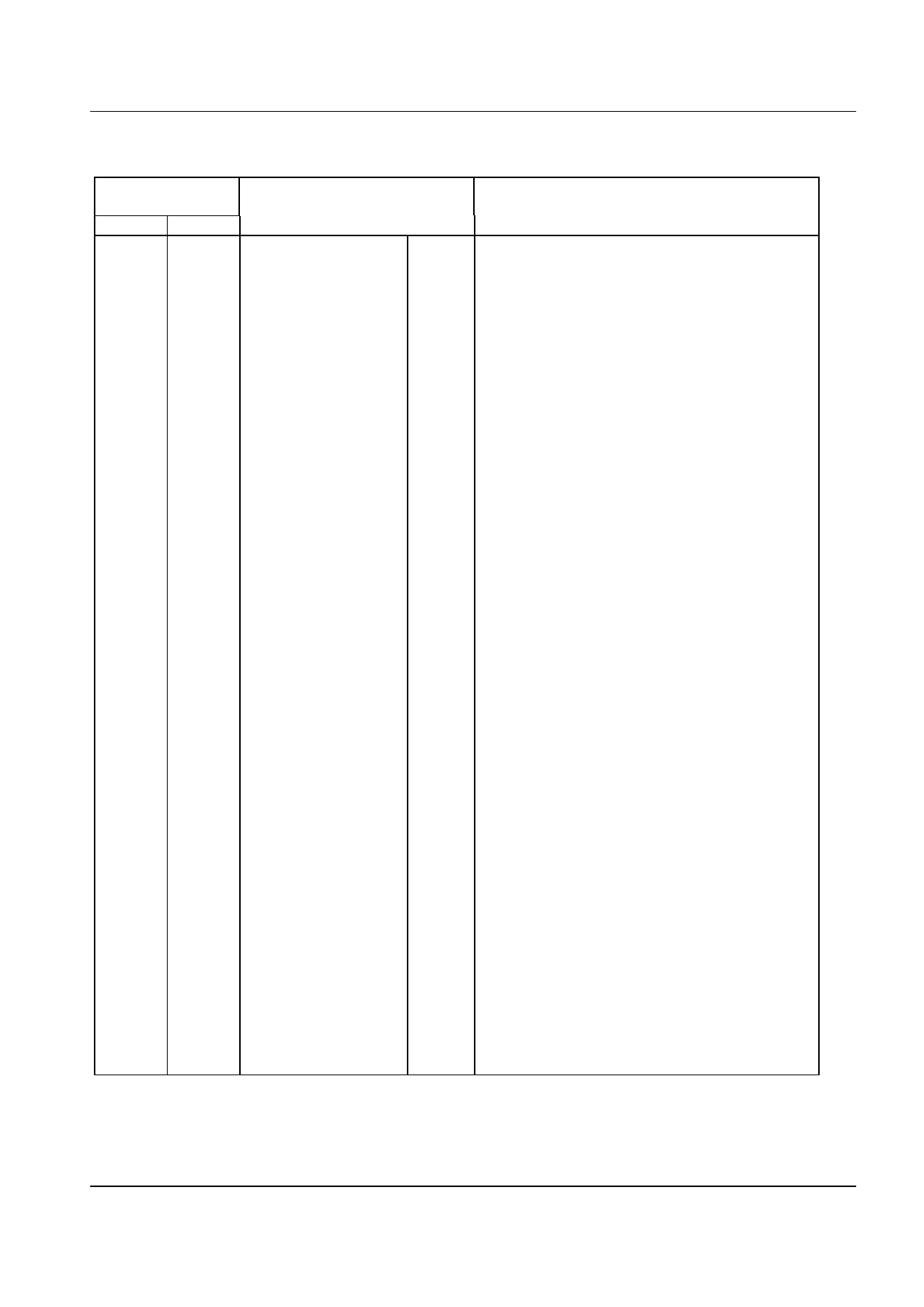
1.3 Signal List (continued)
CMX808A
Package
E3
P4
Signal
Description
Pin No. Pin No.
Name
Type
8
8
NC
9
NC
) No internal connection. Do not make
) any connection to these pins.
9
10 A/D CAP
11 NC
O/P An internal reference voltage for the A to D,
decoupled to VSS by an external capacitor.
No internal connection. Do not make any
connection to this pin.
10
12 Vss
11
13
VBIAS
Power The negative supply rail (ground).
O/P A bias line for the internal circuitry, held at ½
VDD. This pin must be decoupled by a
capacitor mounted close to the device pins.
12
14 RX AMP IN
I/P The inverting input to the Rx input amplifier.
13
15 RX AMP OUT
O/P The output of the Rx input amplifier and the
input to the audio filter section.
14
16 RX AUDIO OUT
O/P Output of the Rx audio filter section.
17 NC
No internal connection. Do not make any
connection to this pin.
15
18 TX AUDIO IN
I/P Input to the Tx audio filter section.
16
19 TX AUDIO OUT
O/P Output of the Tx audio filter section.
17
20 VOLUME IN
I/P Input to the audio volume control.
18
21 TX SUB AUDIO OUT O/P Output of the CTCSS tone generator.
19
22 VOLUME OUT
O/P Output of the audio volume control.
23 NC
No internal connection. Do not make any
connection to this pin.
20
24
VDD
Power The positive supply rail. Levels and voltages
are dependent upon this supply. This pin
should be decoupled to VSS by a capacitor.
Notes: I/P = Input
O/P = Output
© 1999 Consumer Microcircuits Limited
5
D/808A/5
Share Link: 