CGY94 Просмотр технического описания (PDF) - Siemens AG
Номер в каталоге
Компоненты Описание
производитель
CGY94 Datasheet PDF : 9 Pages
| |||
GaAs MMIC
CGY 94
_______________________________________________________________________________________________________
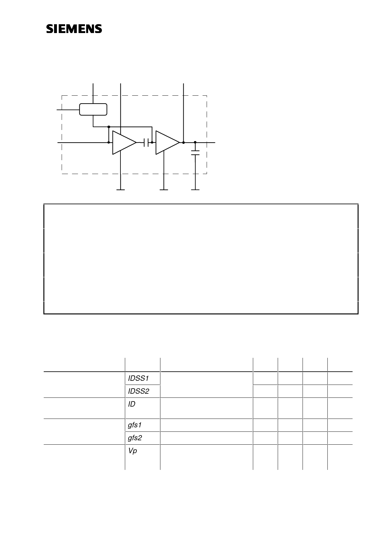
Functional block diagram:
VTR (2)
VG (1)
Control
Circuit
VD1 (7)
Pin (8)
VD2 (12)
Pout (12)
Control circuit:
The drain current ID of the CGY 94 is
adjusted by the internal control circuit.
Therefore a negative voltage (-4V...-6V)
has to be supplied at VG. For transmit
operation VTR must be set to 0V. During
receive operation VTR should be dis-
connected (shut off mode).
GND1 (6, 9)
GND2
(3, 4, 5, 10)
GND3 (11)
Pin #
1
2
3,4,5,10
6,9
7
8
11
12
VG
VTR
GND 2
GND 1
VD1
RFin
GND 3
VD2, RFout
Configuration
Negative voltage at control circuit (-4V...-6V)
Control voltage for transmit mode (0V) or receive mode (open)
RF and DC ground of the 2nd stage
RF and DC ground of the 1st stage
Positive drain voltage of the 1st stage
RF input power
Ground for internal output matching
Positive drain voltage of the 2nd stage, RF output power
DC characteristics
Characteristics
Symbol Conditions
Drain current stage 1 IDSS1 VD=3V, VG=0V, VTR n.c.
stage 2 IDSS2
Drain current with
ID
active current control
VD=3V, VG=-4V, VTR=0V
Transconductance
gfs1
VD=3V, ID=350mA
(stage 1 and 2)
gfs2
VD=3V, ID=700mA
Pinch off voltage
Vp
VD=3V, ID<500µA
(all stages)
min
0.6
2.7
-
0.25
1.1
-3.8
typ
0.9
4.1
1.1
0.32
1.3
-2.8
max
1.3
5.9
-
-
-
-1.8
Unit
A
A
A
S
S
V
Siemens Aktiengesellschaft
pg. 2/9
17.10.95
HL EH PD 21
Share Link: 