SPT9689 Просмотр технического описания (PDF) - Cadeka Microcircuits LLC.
Номер в каталоге
Компоненты Описание
производитель
SPT9689 Datasheet PDF : 8 Pages
| |||

TYPICAL INTERFACE CIRCUIT
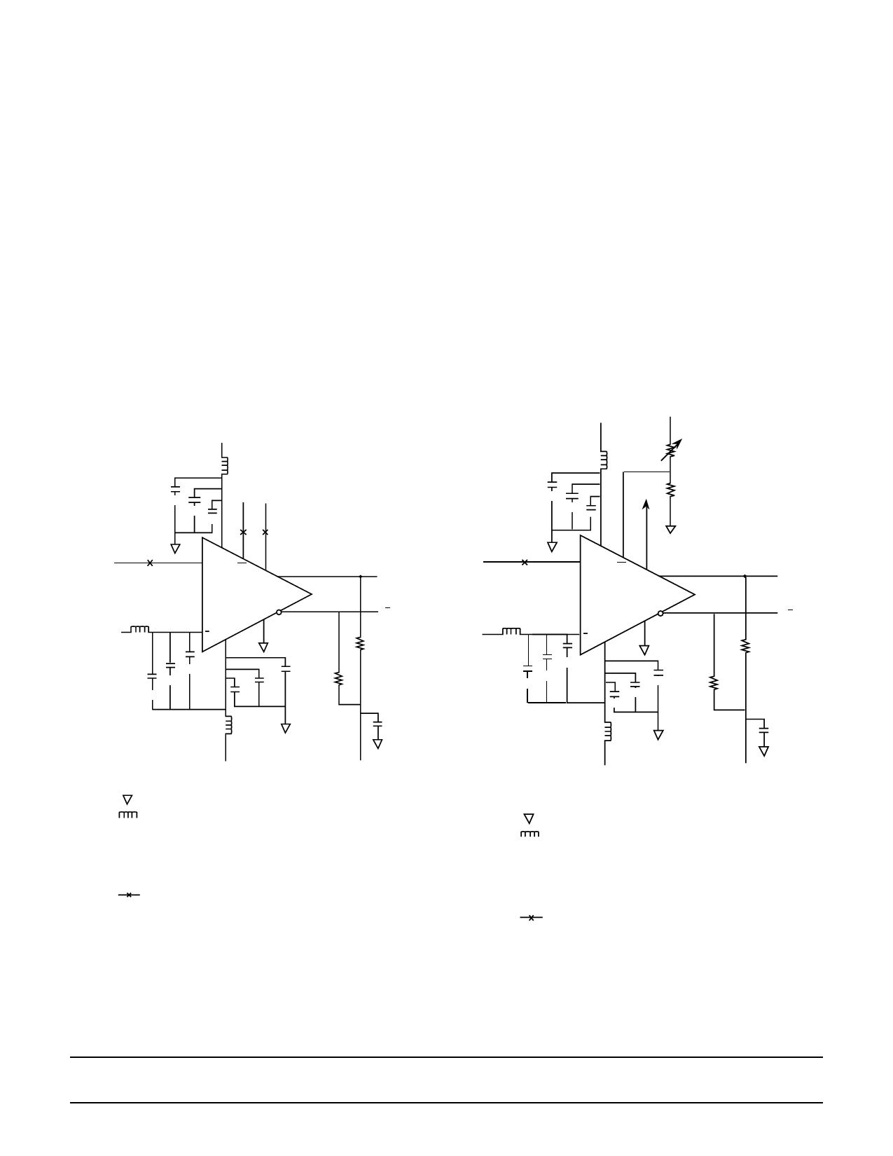
The typical interface circuit using the comparator is shown
in figure 3. Although it needs few external components
and is easy to apply, there are several conditions that
should be noted to achieve optimal performance. The very
high operating speeds of the comparator require careful
layout, decoupling of supplies, and proper design of trans-
mission lines.
Since the SPT9689 comparator is a very high-frequency
and high-gain device, certain layout rules must be fol-
lowed to avoid oscillations. The comparator should be
soldered to the board with component lead lengths kept
as short as possible. A ground plane should be used while
the input impedance to the part is kept as low as possible
to decrease parasitic feedback. If the output board traces
are longer than approximately half an inch, microstripline
techniques must be employed to prevent ringing on the
output waveform. Also, the microstriplines must be termi-
nated at the far end with the characteristic impedance of
the line to prevent reflections. Both supply voltage pins
should be decoupled with high-frequency capacitors as
close to the device as possible. All ground pins and no
connects should be soldered to a common ground plane
to further improve noise immunity. If using the SPT9689
as a single comparator, the outputs of the inactive com-
parator can be grounded, left open, or terminated with
50 ohms to –2 V. All outputs on the active comparator,
whether used or unused, should have identical termina-
tions to minimize ground current switching transients.
Figure 3 – SPT9689 Typical Interface Circuit
+5.0 V
Figure 4 – SPT9689 Typical Interface Circuit
with Hysteresis
+5.0 V
2 V
0 to 200 W
VIN
VREF
10 µF
0.1 µF
100 pF
ECL
+VCC
+
LE
LE
GND
VEE
100 pF
0.1 µF
10 µF
100 pF RL
0.1 µF
50 W
10 µF
Q Output
Q Output
RL
50 W
10 F
5.2 V
2 V
NOTES:
Denotes ground plane.
Ferrite bead. Fair Rite Part # 2643001501.
All resistors are chip type 1%.
0.1 µF and 100 pF capacitors are chip type mounted as close
to the pins as possible.
10 µF tant capacitors have lead lengths <0.25" long.
Represents line termination.
VIN
VREF
10 µF
0.1 µF
100 pF
1.3 V
100 W
+VCC
+
LE
LE
GND
VEE
100 pF
0.1 µF
10 µF
100 pF
0.1 µF
10 µF
RL
50 W
Q Output
Q Output
RL
50 W
10 µF
5.2 V
2 V
NOTES:
Denotes ground plane.
Ferrite bead. Fair Rite Part # 2643001501.
All resistors are chip type 1%.
0.1 µF and 100 pF capacitors are chip type mounted
as close to the pins as possible.
10 µF tant capacitors have lead lengths <0.25" long.
Represents line termination.
SPT9689
6
2/20/01