TH71081 Просмотр технического описания (PDF) - Melexis Microelectronic Systems
Номер в каталоге
Компоненты Описание
производитель
TH71081 Datasheet PDF : 12 Pages
| |||
Not recommended for new designsTH71081
868/915MHz
ASK Transmitter / LO Source
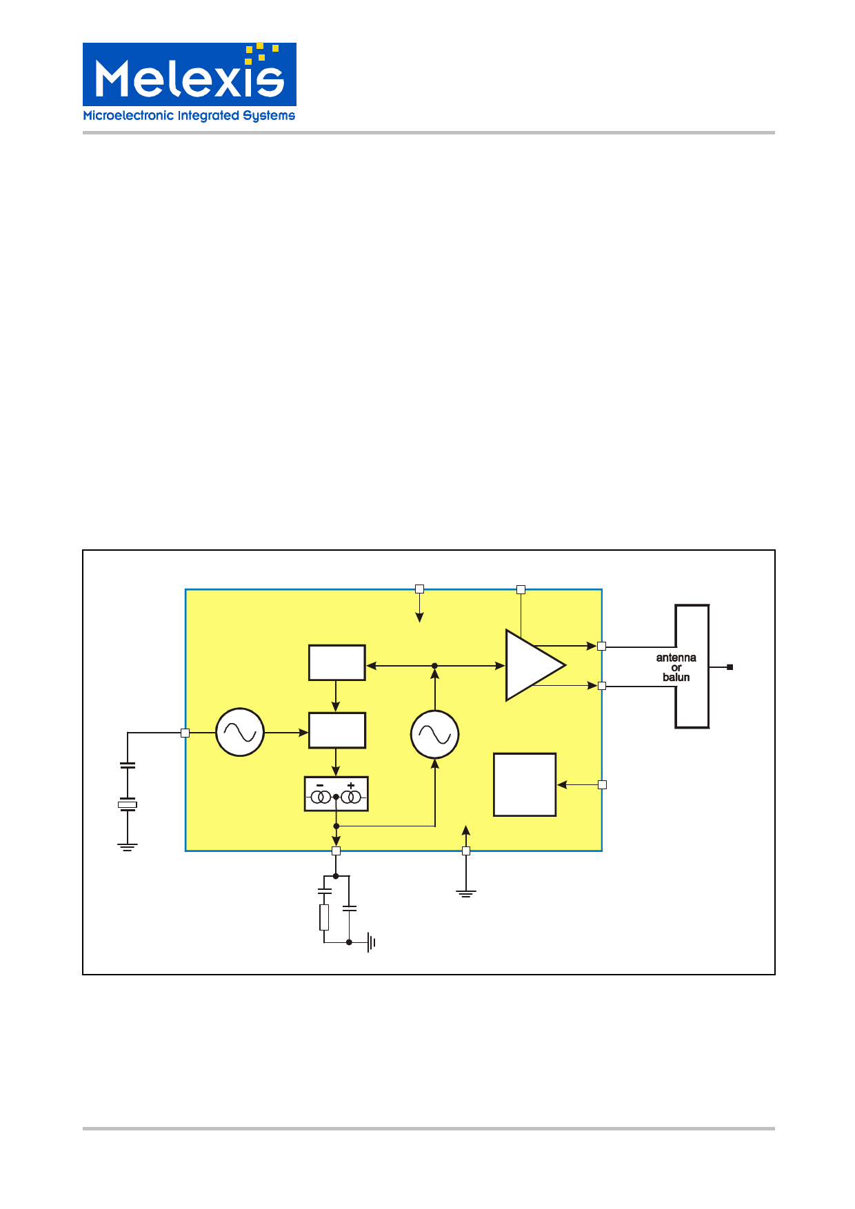
1 Theory of Operation
1.1 General
As depicted in Fig.1, the TH71081 transmitter consists of a fully integrated voltage-controlled oscillator
(VCO), a divide-by-32 divider (div32), a phase-frequency detector (PFD) and a charge pump. An external
loop filter at pin LF determines the dynamic behaviour of the PLL and suppresses reference spurious signals.
The VCO’s output signal feeds the power amplifier (PA). RF signal power Po can be adjusted in six steps
from Po = –15 dBm to +1 dBm either by changing the value of resistor R1 or by varying the voltage VPS at pin
PS/DATA. The open-collector differential output (OUT1, OUT2) can be used to either directly drive a loop
antenna or to be converted to a single-ended impedance by means of a balanced-to-unbalanced (balun)
transformer. For maximum available output power, the differential output should be matched to a load of
about 1 kΩ.
Bandgap biasing ensures stable operation of the IC at a power supply range of 2.2 V to 5.5 V.
1.2 Block Diagram
RO
2
CX1
XTAL
VCC 5
PS/DATA 4
XOSC
div32
PFD
charge
pump
PA
VCO
mode
control
LF 1
CF1
CF2
RF1
8 VEE
OUT1
7
OUT2
6
ENTX
3
VCC
Fig. 1: Block diagram with external components
3901071081
Rev. 009
Page 3 of 12
Data Sheet
May/05
Share Link: 