MC145220DT Просмотр технического описания (PDF) - Freescale Semiconductor
Номер в каталоге
Компоненты Описание
производитель
MC145220DT Datasheet PDF : 27 Pages
| |||
Freescale Semiconductor, Inc.
PIN DESCRIPTIONS
DIGITAL INTERFACE PINS
Din
Serial Data Input (Pin 20)
The bit stream begins with the MSB and is shifted in on the
low–to–high transition of CLK. The bit pattern is 1 byte (8
bits) long to access the C or configuration registers, 2 bytes
(16 bits) to access the first buffer of the R registers, or
3 bytes (24 bits) to access the A registers (see Table 1). The
values in the registers do not change during shifting because
the transfer of data to the registers is controlled by ENB.
NOTE
The value programmed for the N counter must be
greater than or equal to the value of the A counter.
The 13 LSBs of the R registers are double–buffered. As in-
dicated above, data is latched into the first buffer on a 16–bit
transfer. (The 3 MSBs are not double–buffered and have an
immediate effect after a 16–bit transfer.) The two second
buffers of the R register contain the two 13–bit divide ratios
for the R counters. These second buffers are loaded with the
contents of the first buffer as follows. Whenever the A regis-
ter is loaded, the Rs (second) buffer is loaded from the R
(first) buffer. Similarly, whenever the Ai register is loaded, the
Rsi (second) buffer is updated from the R (first) buffer. This
allows presenting new values to the R, A, and N counters
simultaneously. Note that two different R counter divide
ratios may be established: one for the main PLL and another
for PLLi.
The bit stream does not need address bits due to the inno-
vative BitGrabber Plus registers. A steering bit is used to
direct data to either the main PLL or PLLi section of the chip.
Data is retained in the registers over a supply range of 2.7 to
5.5 V. The formats are shown in Figures 14, 15, and 16.
Din typically switches near 50% of V+ to maximize noise
immunity. This input can be directly interfaced to CMOS
devices with outputs guaranteed to switch near rail–to–rail.
When interfacing to NMOS or TTL devices, either a level
shifter (MC74HC14A, MC14504B) or pull–up resistor of 1 kΩ
to 10 kΩ must be used. Parameters to consider when sizing
the resistor are worst–case IOL of the driving device, maxi-
mum tolerable power consumption, and maximum data rate.
CLK
Serial Data Clock Input (Pin 19)
Low–to–high transitions on CLK shift bits available at the
Din pin, while high–to–low transitions shift bits from Output A
(when configured as Data Out, see Pin 10). The 24–1/2
stage shift register is static, allowing clock rates down to dc in
a continuous or intermittent mode.
Eight clock cycles are required to access the C registers.
Sixteen clock cycles are needed for the first buffer of the R
register. Twenty–four cycles are used to access the A regis-
ters. See Table 1 and Figures 14, 15, and 16. The number of
clocks required for cascaded devices is shown in Figures 25
through 27.
CLK typically switches near 50% of V+ and has a Schmitt–
triggered input buffer. Slow CLK rise and fall times are al-
lowed. See the last paragraph of Din for more information.
NOTE
To guarantee proper operation of the power–on
reset (POR) circuit, the CLK pin must be held at
GND (with ENB being a don’t care) or ENB must
be held at the potential of the V+ pin (with CLK be-
ing a don’t care) during power–up. Floating, tog-
gling, or having these pins in the wrong state
during power–up does not harm the chip, but
causes two potentially undesirable effects. First,
the outputs of the device power up in an unknown
state. Second, if two devices are cascaded, the A
Registers must be written twice after power up.
After these two accesses, the two cascaded chips
perform normally.
ENB
Active–Low Enable Input (Pin 11)
This pin is used to activate the serial interface to allow the
transfer of data to/from the device. When ENB is in an inac-
tive high state, shifting is inhibited and the port is held in the
initialized state. To transfer data to the device, ENB (which
must start inactive high) is taken low, a serial transfer is
made via Din and CLK, and ENB is taken back high. The
low–to–high transition on ENB transfers data to the C or A
registers and first buffer of the R register, depending on the
data stream length per Table 1.
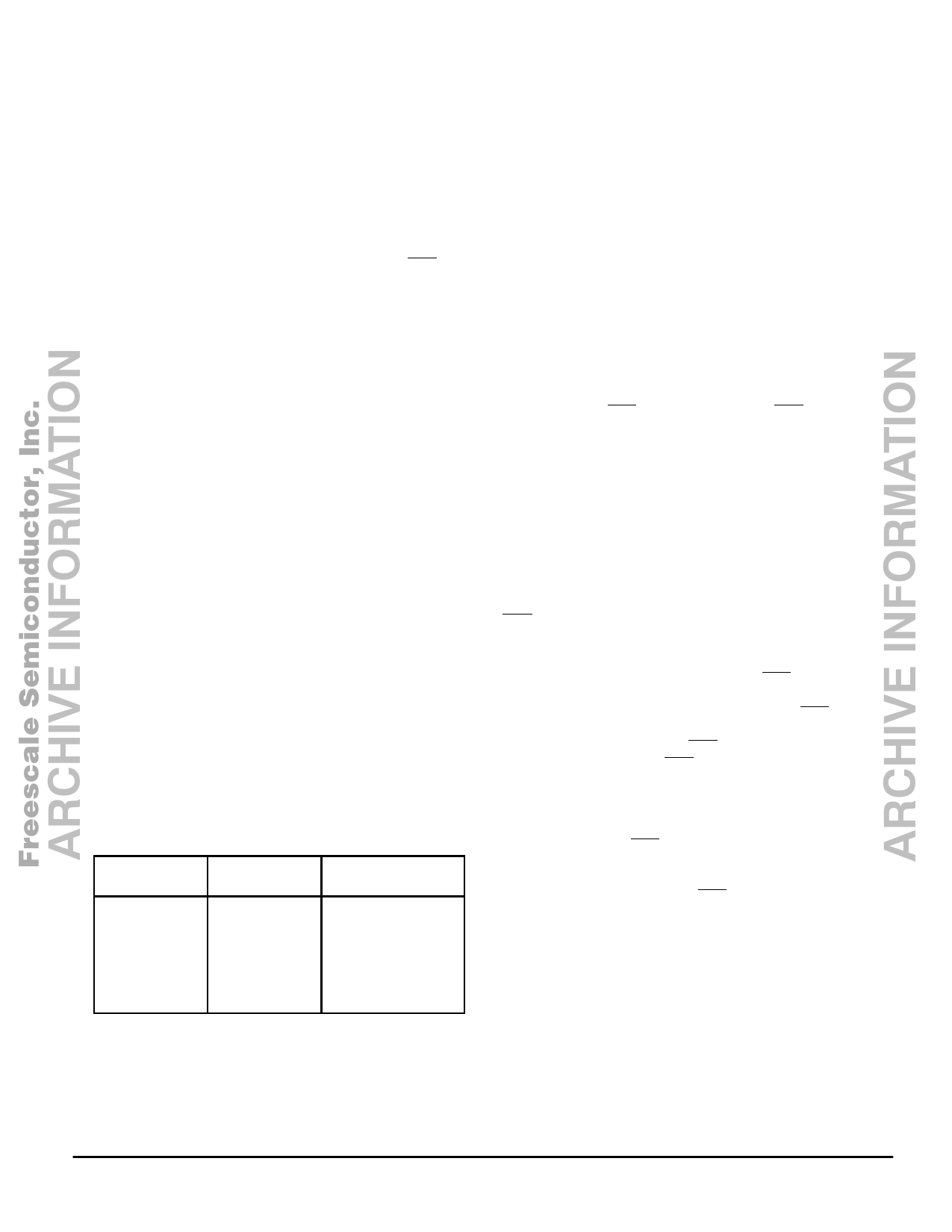
Table 1. Register Access
(MSBs are shifted in first; C0, R0, and A0 are the LSBs)
Number
of Clocks
Accessed
Register
Bit
Nomenclature
8
16
24
Other Values ≤ 32
Values > 32
C Registers
R Register,
First Buffer
A Registers
Not Allowed
See Figures
24 to 27
C7, C6, C5, . . ., C0
R15, R14, R13, . . ., R0
A23, A22, A21, . . ., A0
NOTE
Transitions on ENB must not be attempted while
CLK is high. This puts the device out of synchro-
nization with the microcontroller. Resynchro-
nization occurs whenever ENB is high and CLK is
low.
This input is Schmitt–triggered and switches near 50% of
V+, thereby minimizing the chance of loading erroneous data
into the registers. See the last paragraph of Din for more
information.
For POR information, see the note for the CLK pin.
MOTOROLA WIRELESS SEMICONDUCTOR
SOLUTIONS DEVICE DATA For More Information On This Product,
Go to: www.freescale.com
MC145220
9
Share Link: 