NX25P40-VNI Просмотр технического описания (PDF) - NexFlash -> Winbond Electronics
Номер в каталоге
Компоненты Описание
производитель
NX25P40-VNI
NexFlash -> Winbond Electronics

NX25P40-VNI Datasheet PDF : 28 Pages
| |||
1M / 2M / 4M-BIT SERIAL FLASH MEMORY with 40MHz SPI
NX25P10, NX25P20 AND NX25P40
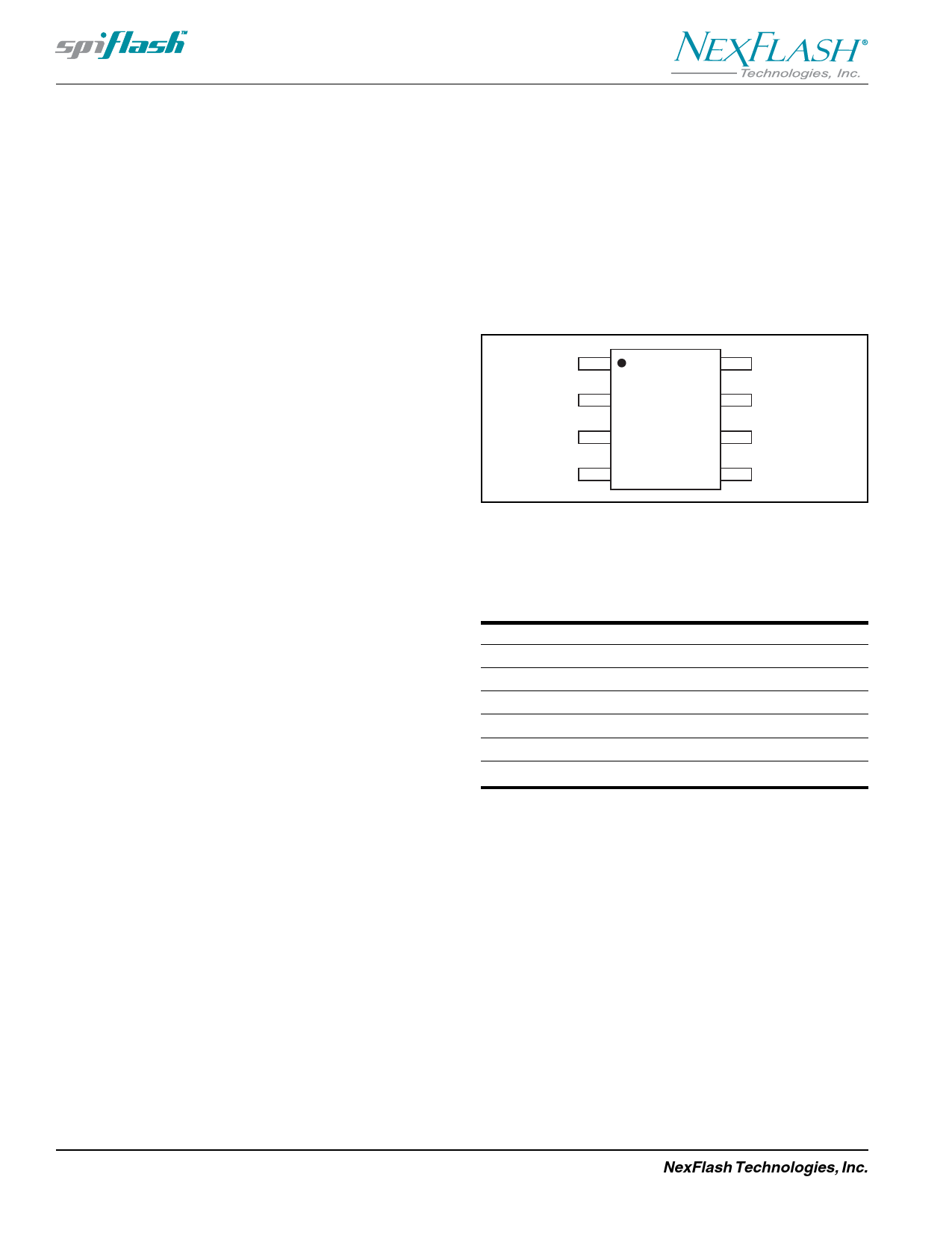
PIN DESCRIPTIONS
Package Types
The standard package for the NX25P10/20/40 is an 8-pin
plastic SOIC with 150 mil body (NexFlash package code N).
It also allows a package migration path to higher density
Serial Flash devices. The pinout for the “N” package is
shown in Figure 2. Package diagrams and dimensions are
illustrated at the end of this data sheet. Optional 8-contact
MLP packages may be available. Please contact NexFlash
for further MLP package information.
Write Protect (WP)
The Write Protect (WP) pin can be used to prevent the
Status Register from being written. Used in conjunction with
the Status Register’s Block Protect (BP0 and BP1) bits and
Status Register Protect (SRP) bits, a portion or the entire
memory array can be hardware protected. The WP pin is
active low.
Serial Data Input (DI)
The SPI Serial Data Input (DI) pin provides a means for
instructions, addresses and data to be serially written to
(shifted into) the device. Data is latched on the rising edge
of the Serial Clock (CLK) input pin.
Serial Data Output (DO)
The SPI Serial Data Output (DO) pin provides a means for
data and status to be serially read from (shifted out of) the
device. Data is shifted out on the falling edge of the Serial
Clock (CLK) input pin.
Serial Clock (CLK)
The SPI Serial Clock Input (CLK) pin provides the timing for
serial input and output operations. ("See SPI "Operations")
Chip Select (CS)
The SPI Chip Select (CS) pin enables and disables device
operation. When CS is high the device is deselected and the
Serial Data Output (DO) pin is at high impedance. When
deselected, the devices power consumption will be at
standby levels unless an internal erase, program or status
register cycle is in progress. When CS is brought low the
device will be selected, power consumption will increase to
active levels and instructions can be written to and data read
from the device. After power-up, CS must transition from
high to low before a new instruction will be accepted. The CS
input must track the Vcc supply level at power-up (see
“Write Protection” and figure 17). If needed a pull-up resister
on CS can be used to accomplish this.
Hold (HOLD)
The HOLD pin allows the device to be paused while it is
actively selected. When HOLD is brought low, while CS is
low, the DO pin will be at high impedance and signals on the
DI and CLK pins will be ignored (don’t care). When
HOLD is brought high, device operation can resume. The
hold function can be useful when multiple devices are
sharing the same SPI signals. (“See Hold function”)
CS
DO
WP
GND
1
8
2
7
3
6
4
5
VCC
HOLD
CLK
DI
Figure 2. NX25P10, NX25P20 and NX25P40 Pin
Assignments, 8-pin SOIC (Package Code N)
Table 1. Pin Descriptions
DI
Data Input
DO
Data Output
CLK
CS
WP
HOLD
Serial Clock Input
Chip Select Input
Write Protect Input
Hold Input
Vcc, GND
Power Supply
6
NexFlash Technologies, Inc.
PRELIMINARY MKP-0009 Rev 6 NXSF040I-0405
04/04/05 ©
Share Link: