NX25P40-VNI Просмотр технического описания (PDF) - NexFlash -> Winbond Electronics
Номер в каталоге
Компоненты Описание
производитель
NX25P40-VNI
NX25P40-VNI Datasheet PDF : 28 Pages
| |||

1M / 2M / 4M-BIT SERIAL FLASH MEMORY with 40MHz SPI
NX25P10, NX25P20 AND NX25P40
INSTRUCTIONS
The instruction set of the NX25P10/20/40 consists of
twelve basic instructions that are fully controlled through the
SPI bus (see Table 3). Instructions are initiated with the
falling edge of Chip Select (CS). The first byte of data
clocked into the DI input provides the instruction code. Data
on the DI input is sampled on the rising edge of clock with
most significant bit (MSB) first.
feature further protects the device from inadvertent writes.
Additionally, while the memory is being programmed or
erased, or when the Status Register is being written, all
instructions except for Read Status Register will be ignored
until the program or erase cycle has completed.
Instructions vary in length from a single byte to several
bytes and may be followed by address bytes, data bytes,
dummy bytes (don’t care), and in some cases, a combina-
tion. Instructions are completed with the rising edge of edge
CS. Clock relative timing diagrams for each instruction are
included in figures 5 through 17. All read instructions can be
completed after any clocked bit. However, all instructions
that Write, Program or Erase must complete on a byte
boundary (CS driven high after a full 8-bits have been
clocked) otherwise the instruction will be terminated. This
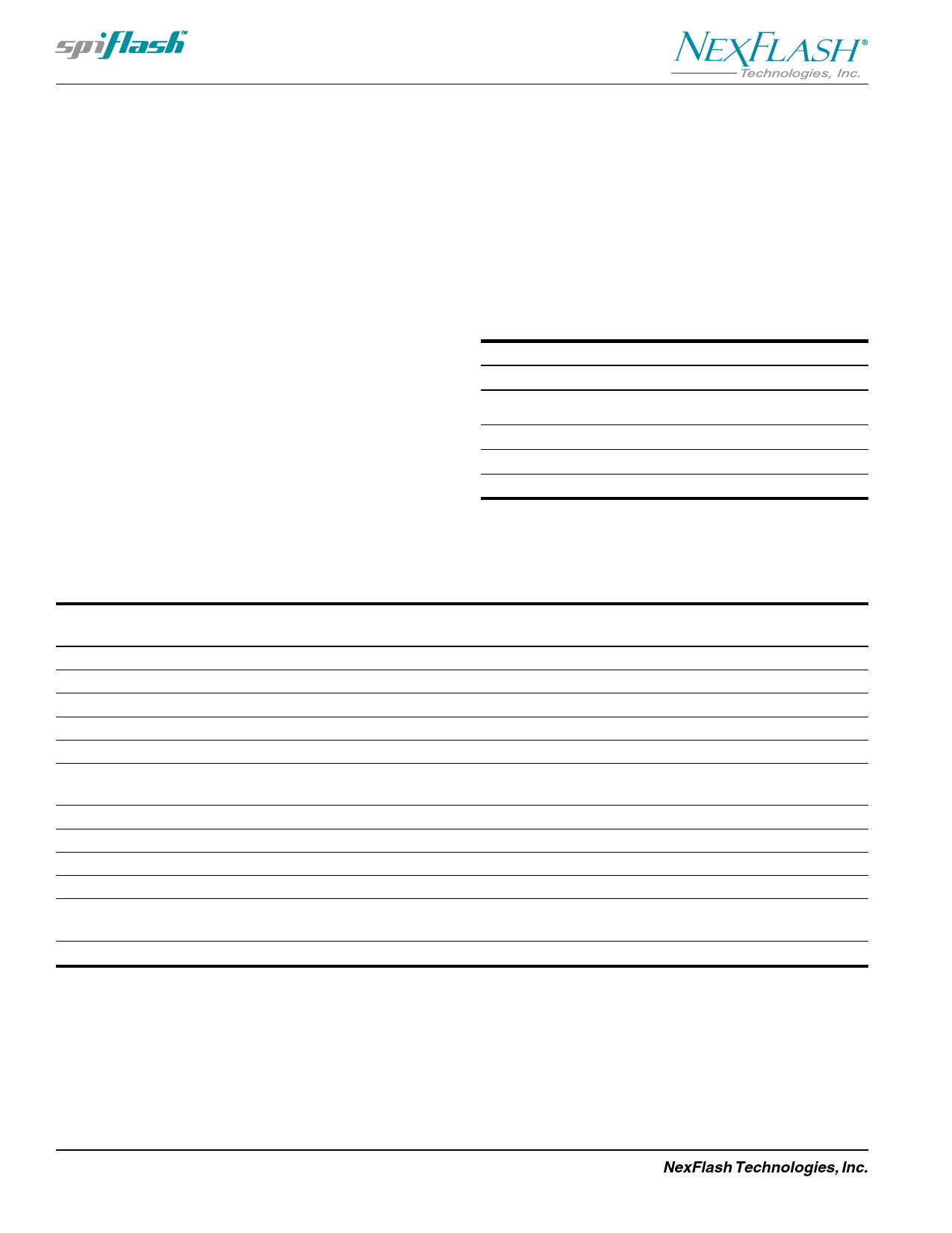
Table 4: Manufacturer and Device Identification
Manufacturer ID
(M7-M0)
NexFlash
EFh
Device ID
NX25P10
NX25P20
NX25P40
(ID7-ID0)
10h
11h
12h
Table 3: Instruction Set (1)
Instruction Name
Write Enable
Write Disable
Read Status Register
Write Status Register
Read Data
Fast Read
Page Program
Sector Erase
Bulk Erase
Power-down
Release Power-down
and Device ID
Manufacturer/Device ID
Byte 1
Code
06h
04h
05h
01h
03h
0Bh
Byte 2 (5)
(S7–S0)(1)
S7–S0
A23–A16
A23–A16
Byte 3
A15–A8
A15–A8
Byte 4
A7–A0
A7–A0
Byte 5 Byte 6
(D7–D0) (Next byte)
dummy (D7–D0)
02h
A23–A16 A15–A8 A7–A0 (D7–D0) (Next byte)
D8h
A23–A16 A15–A8 A7–A0(6)
C7h
B9h
ABh dummy dummy dummy (ID7-ID0)
90h
dummy dummy 00h
(M7-M0) (ID7-ID0)
n-Bytes
(2)
continuous
(Next Byte)
continuous
up to 256 bytes
(3)
(4)
Notes:
1. Data bytes are shifted with Most Significant Bit first. Byte fields with data in parenthesis “( )” indicate data being read from
the device on the DO pin.
2. The Status Register contents will repeat continuously until CS terminate the instruction.
3. The Device ID will repeat continuously until CS terminate the instruction.
4. The Manufacturer ID and Device ID bytes will repeat continuously until CS terminate the instruction.
5. Unused upper address bits must be set to a 0 for the NX25P10.
6. The lowest 16 address bits (A15-A0) must be set to 0.
10
NexFlash Technologies, Inc.
PRELIMINARY MKP-0009 Rev 6 NXSF040I-0405
04/04/05 ©