GS74104AJ-7 Просмотр технического описания (PDF) - Giga Semiconductor
Номер в каталоге
Компоненты Описание
производитель
GS74104AJ-7 Datasheet PDF : 12 Pages
| |||
GS74104ATP/J
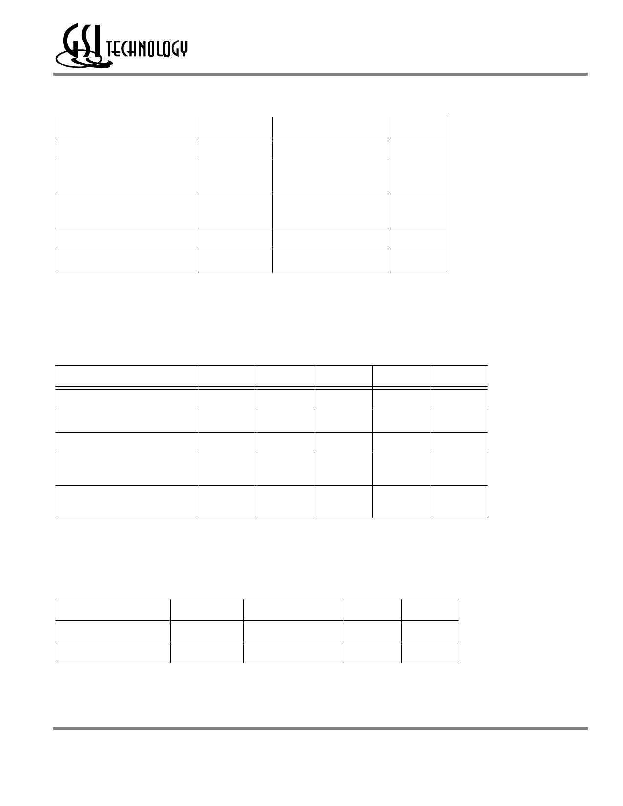
Absolute Maximum Ratings
Parameter
Symbol
Rating
Unit
Supply Voltage
VDD
Input Voltage
VIN
Output Voltage
VOUT
Allowable power dissipation
PD
Storage temperature
TSTG
–0.5 to +4.6
V
–0.5 to VDD +0.5
V
(≤ 4.6 V max.)
–0.5 to VDD +0.5
(≤ 4.6 V max.)
V
0.7
W
–55 to 150
oC
Note:
Permanent device damage may occur if Absolute Maximum Ratings are exceeded. Functional operation shall be restricted to Rec-
ommended Operating Conditions. Exposure to higher than recommended voltages for extended periods of time could affect device
reliability.
Recommended Operating Conditions
Parameter
Symbol Min
Supply Voltage for -7/-8/-10/-12
VDD
3.0
Input High Voltage
VIH
2.0
Input Low Voltage
VIL
–0.3
Ambient Temperature,
Commercial Range
TAc
0
Ambient Temperature,
Industrial Range
TAI
–40
Typ
Max
Unit
3.3
3.6
V
—
VDD +0.3
V
—
0.8
V
—
70
oC
—
85
oC
Notes:
1. Input overshoot voltage should be less than VDD +2 V and not exceed 20 ns.
2. Input undershoot voltage should be greater than –2 V and not exceed 20 ns.
Capacitance
Parameter
Symbol
Test Condition
Max
Unit
Input Capacitance
CIN
VIN = 0 V
5
pF
Output Capacitance
COUT
VOUT = 0 V
7
pF
Notes:
1. Tested at TA = 25°C, f = 1 MHz
2. These parameters are sampled and are not 100% tested.
Rev: 1.03b 10/2002
3/12
© 2001, Giga Semiconductor, Inc.
Specifications cited are subject to change without notice. For latest documentation see http://www.gsitechnology.com.
Share Link: 