FT8010 Просмотр технического описания (PDF) - ON Semiconductor
Номер в каталоге
Компоненты Описание
производитель
FT8010 Datasheet PDF : 15 Pages
| |||
Functional Description
The FT8010 reset timer uses an internal oscillator and a
two-stage, 21-bit counter to determine when the output
pins switch. Time N is set by the hard-wired logic level
of the DSR pin. N is either 7.5 ±20% seconds for
DSR=LOW or 11.25 ±20% seconds for DSR=HIGH.
Table 1. FT8010 Truth Table
DSR
Reset Timer ( +-20% )
0
7.50s
1
11.25s
The two input pins, /SR0 and /SR1, drive voltage
comparators that compare the voltage on the input with
the voltage set by the reference block. A low input signal
on both /SR0 and /SR1 starts the oscillator. The
oscillator sends data pulses to the digital core, which
includes the counter. There are two scenarios for
counting, as described below: short duration and long
duration. In the short-duration scenario, outputs /RST1
and RST2 are not affected. In the long duration
scenario, the outputs change state after time N. The
outputs return to their original states when a HIGH input
signal occurs on either /SR0 or /SR1.
The /RST1 output is an open-drain driver. When the count
time exceeds time N, the /RST1 output drives LOW. The
RST2 output is a push-pull driver. When the count time
exceeds time N, the RST2 output drives HIGH.
The TRIG pin should be tied GND or LOW during
normal operation. The TRIG pin is a test mode pin used
for SCAN testing.
Application Note
IMPORTANT: The DSR pin must be tied to VCC or GND
to provide a HIGH or LOW voltage level. The voltage
level on the DSR pin determines the length of the
configurable delay. It is important that the voltage level
on the DSR pin not change during normal operation.
The DSR pin must be tied directly to VCC or GND before
SR0 or SR1 buttons go LOW. Do not use pull-up or pull-
down resistors on the DSR pin.
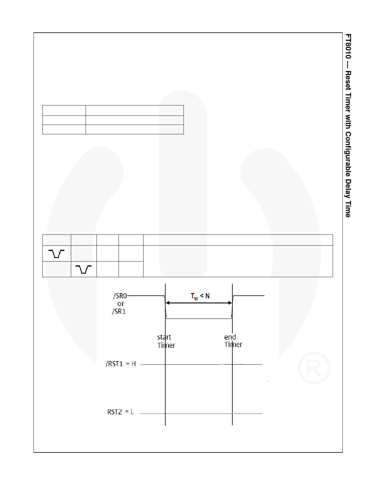
Short Duration (tW < N)
In this case, both input /SR0 and /SR1 are LOW for a
duration tW which is shorter than time N. When an input
goes LOW, the internal timer starts counting. The input
goes HIGH before time N. The timer stops counting and
resets and no changes occur on the outputs (see Figure 4).
/SR0
L
/SR1 /RST1 /RST2
Description
L
H
L The timer starts counting when both inputs go LOW. The timer stops
counting and resets when either input goes HIGH. No changes occur on the
H
L outputs, Both /SR0 and /SR1 need to be LOW to activate (start) the timer.
© 2009 Fairchild Semiconductor Corporation
FT8010 • Rev. 1.0.8
Figure 4. Short Duration Waveform
4
www.fairchildsemi.com
Share Link: 