SMS2916 Просмотр технического описания (PDF) - Summit Microelectronics
Номер в каталоге
Компоненты Описание
производитель
SMS2916 Datasheet PDF : 14 Pages
| |||
SMS2902/SMS2904/SMS2916
ABSOLUTE MAXIMUM RATINGS
Temperature Under Bias ............................................................................................................................... -40°C to +85°C
Storage Temperature ..................................................................................................................................... -65°C to +125°C
Soldering Temperature (less than 10 seconds) ................................................................................................................... 300°C
Supply Voltage ............................................................................................................................................................. 0 to 6.5V
Voltage on Any Pin ....................................................................................................................................... -0.3V to VCC+0.3V
ESD Voltage (JEDEC method) .......................................................................................................................................... 2,000V
NOTE: These are STRESS ratings only. Appropriate conditions for operating these devices are given elsewhere in this specification. Stresses
beyond those listed here may permanently damage the part. Prolonged exposure to maximum ratings may affect device reliability.
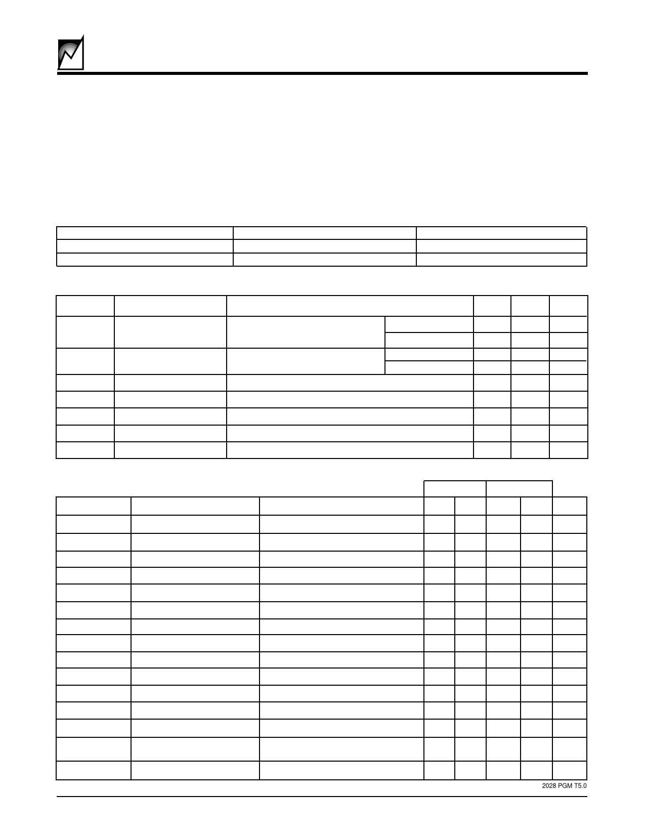
RECOMMENDED OPERATING CONDITIONS
Temperature
Min
Commercial
0°C
Max
+70°C
Industrial
-40°C
+85°C
2028 PGM T3.0
DC ELECTRICAL CHARACTERISTICS (over recommended operating conditions unless otherwise specified)
Symbol
Parameter
Conditions
Min
Max Units
SCL = CMOS Levels @ 100KHz
VCC =5.5V
ICC
Supply Current (CMOS)
SDA = Open
All other inputs = GND or VCC
VCC =3.3V
ISB
Standby Current (CMOS) SCL = SDA = VCC
All other inputs = GND
VCC =5.5V
VCC =3.3V
ILI
Input Leakage
VIN = 0 To VCC
3
mA
2
mA
50
µA
25
µA
10
µA
ILO
Output Leakage
VOUT = 0 To VCC
VIL
Input Low Voltage
S0, S1, S2, SCL, SDA, RESET#
10
µA
0.3xVCC V
VIH
Input High Voltage
S0, S1, S2, SCL, SDA, RESET
0.7xVCC
V
VOL
Output Low Voltage
IOL = 3mA SDA
AC ELECTRICAL CHARACTERISTICS
(over recommended operating conditions unless otherwise specified)
2.7V to 4.5V
0.4
V
2028 PGM T4.0
4.5V to 5.5V
Symbol
Parameter
Conditions
Min Max Min Max Units
fSCL
tLOW
tHIGH
tBUF
tSU:STA
tHD:STA
tSU:STO
tAA
tDH
tR
tF
tSU:DAT
tHD:DAT
TI
tWR
SCL Clock Frequency
Clock Low Period
Clock High Period
Bus Free Time
Start Condition Setup Time
Start Condition Hold Time
Stop Condition Setup Time
Clock to Output
Data Out Hold Time
SCL and SDA Rise Time
SCL and SDA Fall Time
Data In Setup Time
Data In Hold Time
Noise Spike Width
@ SCL, SDA Inputs
Write Cycle Time
Before New Transmission
SCL Low to SDA Data Out Valid
SCL Low to SDA Data Out Change
Noise Suppression Time Constant
3
0
100
4.7
1.3
4.0
0.6
4.7
1.3
4.7
0.6
4.0
0.6
4.7
0.6
0.3 3.5 0.2
0.3
0.2
1000
300
250
100
0
0
100
400 KHz
µs
µs
µs
µs
µs
µs
0.9 µs
µs
300 ns
300 ns
ns
ns
100 ns
10
10 ms
2028 PGM T5.0
2028 5.0 4/18/00
Share Link: 