USB3300-EZK(2005) Просмотр технического описания (PDF) - SMSC -> Microchip
Номер в каталоге
Компоненты Описание
производитель
USB3300-EZK Datasheet PDF : 11 Pages
| |||
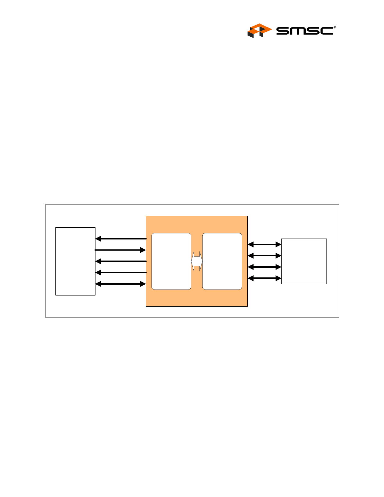
Hi-Speed USB Host or Device PHY with ULPI Low Pin Interface
Table 1 USB3300 Pin Definitions (continued)
DIRECTION, ACTIVE
PIN
NAME
TYPE
LEVEL DESCRIPTION
5
ID
Input,
Analog
N/A ID pin of the USB cable. For non-OTG applications
this pin can be floated. For an A-Device ID = 0. For
a B-Device ID = 1.
6
VDD3.3
Power
N/A 3.3V Supply. A 0.1uF bypass capacitor should be
connected between this pin and the ground plane on
the PCB.
7
DP
I/O,
Analog
N/A D+ pin of the USB cable.
8
DM
I/O,
Analog
N/A D- pin of the USB cable.
9
RESET
Input, CMOS High Optional active high transceiver reset. This is the
same as a write to the ULPI Reset, address 04h, bit
5. This does not reset the ULPI register set. This
signal must be de-asserted synchronous to
CLKOUT. This pin includes an integrated pull-down
resistor to ground. If not used this pin can be floated
or connected to ground (recommended).
10
EXTVBUS
Input, CMOS High External Vbus Detect. Connect to fault output of an
external USB power switch or an external Vbus Valid
comparator.
11
NXT
Output,
CMOS
High
The PHY asserts NXT to throttle the data. When the
Link is sending data to the PHY, NXT indicates when
the current byte has been accepted by the PHY. The
Link places the next byte on the data bus in the
following clock cycle.
12
DIR
Output,
CMOS
N/A Controls the direction of the data bus. When the
PHY has data to transfer to the Link, it drives DIR
high to take ownership of the bus. When the PHY
has no data to transfer it drives DIR low and
monitors the bus for commands from the Link. The
PHY will pull DIR high whenever the interface cannot
accept data from the Link, such as during PLL start-
up.
13
STP
Input,
CMOS
High
The Link asserts STP for one clock cycle to stop the
data stream currently on the bus. If the Link is
sending data to the PHY, STP indicates the last byte
of data was on the bus in the previous cycle.
14
CLKOUT
Output,
CMOS
N/A 60MHz reference clock output. All ULPI signals are
driven synchronous to the rising edge of this clock.
15
VDD1.8
Power
N/A 1.8V digital supply. A 0.1uF bypass capacitor to
ground is recommended. This pin should be
connected to the other VDD1.8, pin 26.
16
VDD3.3
Power
N/A A 0.1uF bypass capacitor should be connected
between this pin and the ground plane on the PCB.
SMSC USB3300
7
PRODUCT PREVIEW
Revision 1.02 (02-16-05)
Share Link: 