EVAL-AD5755-1SDZ Просмотр технического описания (PDF) - Analog Devices
Номер в каталоге
Компоненты Описание
производитель
EVAL-AD5755-1SDZ
Analog Devices

EVAL-AD5755-1SDZ Datasheet PDF : 45 Pages
| |||
Data Sheet
AD5757
AC PERFORMANCE CHARACTERISTICS
AVDD = VBOOST_x = 15 V; DVDD = 2.7 V to 5.5 V; AVCC = 4.5 V to 5.5 V; dc-to-dc converterdisabled; AGND = DGND = GNDSWx = 0 V;
REFIN = 5 V; RL = 300 Ω; all specifications TMIN to TMAX, unless otherwise noted.
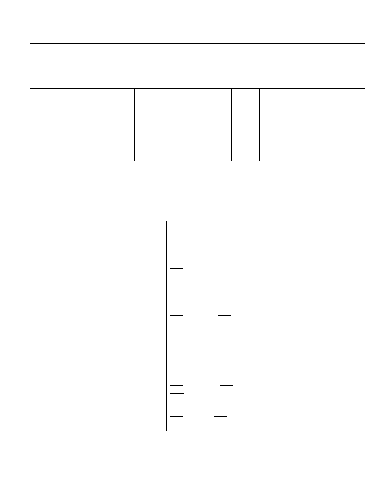
Table 2.
Parameter 1
DYNAMIC PERFORMANCE
Current Output
Output Current Settling Time
Output Noise (0.1 Hz to 10 Hz
Bandwidth)
Output Noise Spectral Density
Min Typ
Max
Unit
Test Conditions/Comments
15
See test conditions/
comments
0.15
0.5
µs
To 0.1% FSR (0 mA to 24 mA)
ms
See Figure 27, Figure 28, and Figure 29
LSB p-p 16-bit LSB, 0 mA to 24 mA range
nA/√Hz Measured at 10 kHz, midscale output,
0 mA to 24 mA range
1 Guaranteed by design and characterization; not production tested.
TIMING CHARACTERISTICS
AVDD = V = BOOST_x 15 V; DVDD = 2.7 V to 5.5 V; AVCC = 4.5 V to 5.5 V; dc-to-dc converterdisabled; AGND = DGND = GNDSWx = 0 V;
REFIN = 5 V; RL = 300 Ω; all specifications TMIN to TMAX, unless otherwise noted.
Table 3.
Parameter 1, 2, 3
t1
t2
t3
t4
t5
t6
t7
t8
t9
t10
t11
t12
t13
t14
t15
t16
t17
t18
t19
Limit at TMIN, TMAX
33
13
13
13
13
198
5
5
5
20
Unit
ns min
ns min
ns min
ns min
ns min
ns min
µs min
ns min
ns min
µs min
5
10
500
See the AC Performance
Characteristics section
10
5
40
5
500
800
20
µs min
ns min
ns max
µs max
ns min
µs max
ns max
µs min
ns min
ns min
µs min
5
µs min
Description
SCLK cycle time
SCLK high time
SCLK low time
SYNC falling edge to SCLK falling edge setup time
24th/32nd SCLK falling edge to SYNC rising edge (see Figure 55)
SYNC high time after a configuration write
SYNC high time after a DAC update write
Data setup time
Data hold time
SYNC rising edge to LDAC falling edge (applies to any channel that has digital
slew rate control enabled) (single DAC updated)
SYNC rising edge to LDAC falling edge (single DAC updated)
LDAC pulse width low
LDAC falling edge to DAC output response time
DAC output settling time
CLEAR high time
CLEAR activation time
SCLK rising edge to SDO valid
SYNC rising edge to DAC output response time (LDAC = 0) (single DAC updated)
LDAC falling edge to SYNC rising edge
RESET pulse width
SYNC high to next SYNC low (digital slew rate controlenabled) (single DAC
updated)
SYNC high to next SYNC low (digital slew rate controldisabled) (single DAC
updated)
1 Guaranteed by design and characterization; not production tested.
2 All input signals are specified with tRISE = tFALL = 5 ns (10% to 90% of DVDD) and timed from a voltage level of 1.2 V.
3 See Figure 3, Figure 4, Figure 6, and Figure 7.
Rev. G | Page 7 of 45
Share Link: