EL2142 Просмотр технического описания (PDF) - Renesas Electronics
Номер в каталоге
Компоненты Описание
производитель
EL2142 Datasheet PDF : 6 Pages
| |||
EL2142
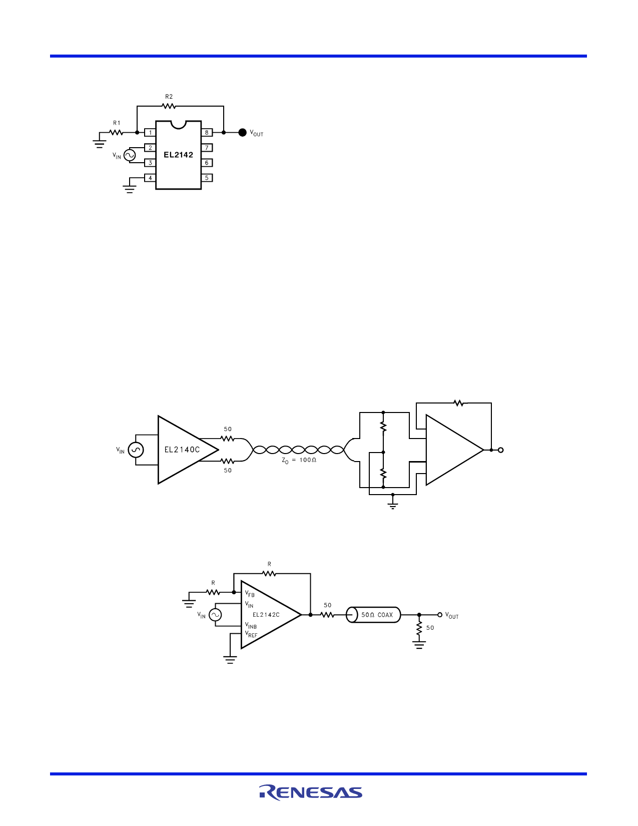
Applications Information
Gain Equation
VOUT = ((R2+R1)/R1) x (VIN-VINB+VREF) when R1 tied to
GND
VOUT = ((R2+R1)/R1) x (VIN-VINB) when R1 tied to VREF
Choice of Feedback Resistor
For a gain of one, VOUT may be shorted back to VFB, but
100-200 improves the bandwidth. For gains greater than
Typical Applications Circuits
one, there is little to be gained from choosing resistor R1
value below 200, for it would only result in increased power
dissipation and potential signal distortion. Above 200, the
bandwidth response will develop some peaking (for a gain of
one), but substantially higher R1 values may be used for
higher voltage gains, such as up to 1k at a gain of four
before peaking will develop.
Capacitance Considerations
As with many high bandwidth amplifiers, the EL2142 prefers
not to drive highly capacitive loads. It is best if the
capacitance on VOUT is kept below 10pF if the user does not
want gain peaking to develop. The VFB node forms a
potential pole in the feedback loop, so capacitance should
be minimized on this node for maximum bandwidth.
The amount of capacitance tolerated on any of these nodes
in an actual application will also be dependent on the gain
setting and the resistor values in the feedback network.
100
50
VFB
VIN
EL2142
VINB
50
VREF
VOUT
FIGURE 1. TYPICAL TWISTED PAIR APPLICATION
FIGURE 2. COAXIAL CABLE DRIVER PAIR APPLICATION
FN7049 Rev 1.00
February 11, 2005
Page 4 of 6
Share Link: 