CY7C1061DV33-10BV1XI –Я—А–Њ—Б–Љ–Њ—В—А —В–µ—Е–љ–Є—З–µ—Б–Ї–Њ–≥–Њ –Њ–њ–Є—Б–∞–љ–Є—П (PDF) - Cypress Semiconductor
–Э–Њ–Љ–µ—А –≤ –Ї–∞—В–∞–ї–Њ–≥–µ
–Ъ–Њ–Љ–њ–Њ–љ–µ–љ—В—Л –Ю–њ–Є—Б–∞–љ–Є–µ
–њ—А–Њ–Є–Ј–≤–Њ–і–Є—В–µ–ї—М
CY7C1061DV33-10BV1XI Datasheet PDF : 18 Pages
| |||
CY7C1061DV33
Switching Waveforms (continued)
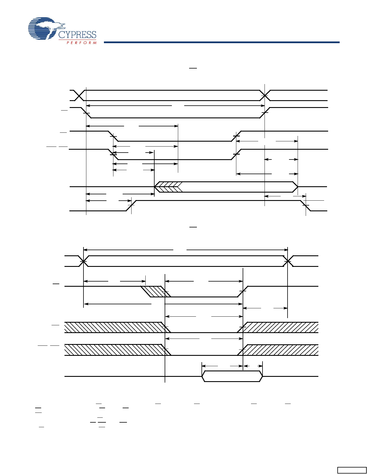
Figure 8. Read Cycle No. 2 (OE Controlled) [19, 20, 21]
Address
CE
OE
BHE, BLE
Data Out
VCC
Supply
Current
Address
CE
WE
BHE, BLE
Data I/O
tRC
tACE
tDOE
tLZOE
tDBE
tLZBE
High Impedance
tLZCE
tPU
50%
Data Valid
tHZOE
tHZCE
tHZBE
High
Impedance
tPD
50%
IICCCC
IISSBB
Figure 9. Write Cycle No. 1 (CE Controlled) [19, 22, 23]
tWC
tSA
tSCE
tAW
tHA
tPWE
tBW
tSD
tHD
Notes
19.
For
CE
all packages
is HIGH. For
except
-BV1XI
-BV1XI, CE is the logical combination
package, CE refers to CE.
of
CE1
and
CE2.
When
CE1
is
LOW
and
CE2
is
HIGH,
CE
is
LOW;
when
CE1
is
HIGH
or
CE2
is
LOW,
20. WE is HIGH for read cycle.
21. Address valid before or similar to CE transition LOW.
22. Data I/O is high impedance if OE, BHE, and/or BLE = VIH.
23. If CE goes HIGH simultaneously with WE going HIGH, the output remains in a high-impedance state.
Document Number: 38-05476 Rev. *H
Page 9 of 17
[+] Feedback
Share Link: 