CXD2467AQ Просмотр технического описания (PDF) - Sony Semiconductor
Номер в каталоге
Компоненты Описание
производитель
CXD2467AQ Datasheet PDF : 38 Pages
| |||
CXD2467AQ
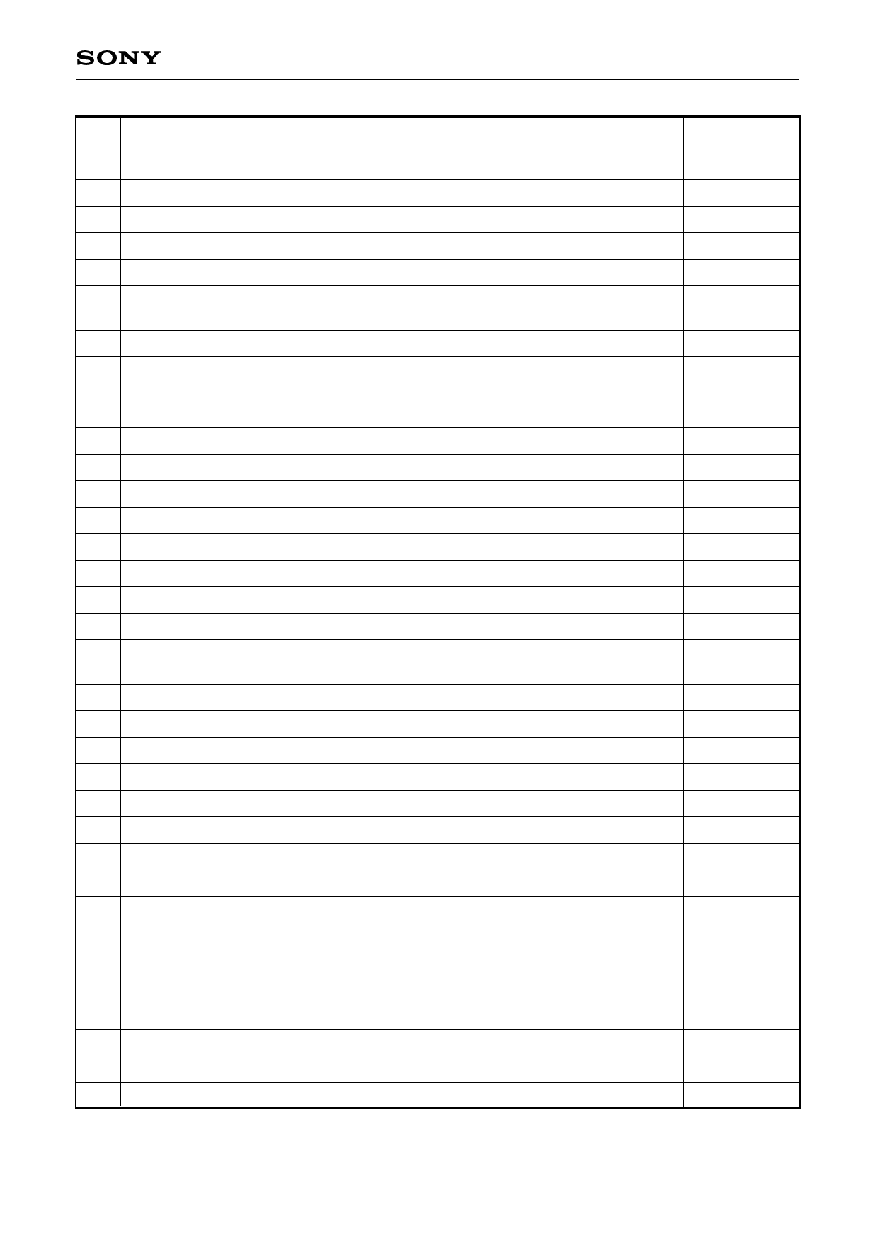
Pin
No.
Symbol
33 CLKOUT
34 Vss
35 CLKSEL1
36 CLKSEL2
37 CLKPOL1
38 HDIN2
39 HDPOL2
40 CLK3P
41 CLK3N
42 VDD
43 VSS
44 CLK3C
45 VSS
46 CLK4
47 CLKSEL3
48 CLKSEL4
49 CLKPOL2
50 IRRET
51 HRET
52 VSS
53 XCLR
54 VDD
55 VSS
56 B2OUT0
57 B2OUT1
58 B2OUT2
59 B2OUT3
60 B2OUT4
61 B2OUT5
62 B2OUT6
63 B2OUT7
64 B2OUT8
65 B2OUT9
Input pin
I/O
Description
processing
for open status
O 1/2 frequency-divided clock output
—
— GND
—
I Input clock selection (High: CLK1C, Low: CLK1P, N)
L
I Input clock selection (High: CLK2, Low: CLK1)
L
I
1/2 frequency division circuit output selection
(High: XQ output, Low: Q output)
L
I Horizontal sync signal input-2
—
I
HDIN2 input polarity selection
(High: positive polarity, Low: negative polarity)
L
I Clock input-2 (small-amplitude differential input, positive polarity)
—
I Clock input-2 (small-amplitude differential input, negative polarity)
—
— Power supply
—
— GND
—
I Clock input-2 (CMOS input)
—
— GND
—
I 1/2 frequency-divided clock input-2 (CMOS input)
—
I Input clock selection (High: CLK3C, Low: CLK3P, N)
L
I Input clock selection (High: CLK4, Low: CLK3)
L
I
1/2 frequency division circuit output selection
(High: XQ output, Low: Q output)
L
O Auxiliary pulse output
—
O Auxiliary pulse output
—
— GND
—
I External clear (Low: reset)
H
— Power supply
—
— GND
—
O Blue data output (port 2)
—
O Blue data output (port 2)
—
O Blue data output (port 2)
—
O Blue data output (port 2)
—
O Blue data output (port 2)
—
O Blue data output (port 2)
—
O Blue data output (port 2)
—
O Blue data output (port 2)
—
O Blue data output (port 2)
—
O Blue data output (port 2)
—
–5–
Share Link: 