IRF9540 Просмотр технического описания (PDF) - Harris Semiconductor
Номер в каталоге
Компоненты Описание
производитель
IRF9540 Datasheet PDF : 11 Pages
| |||
IRF9540, IRF9541, IRF9542, IRF9543, RF1S9540, RF1S9540SM
Electrical Specifications TC = 25oC, Unless Otherwise Specified (Continued)
PARAMETERS
SYMBOL
TEST CONDITIONS
MIN
Internal Drain Inductance
Internal Source Inductance
LD
Measured From the
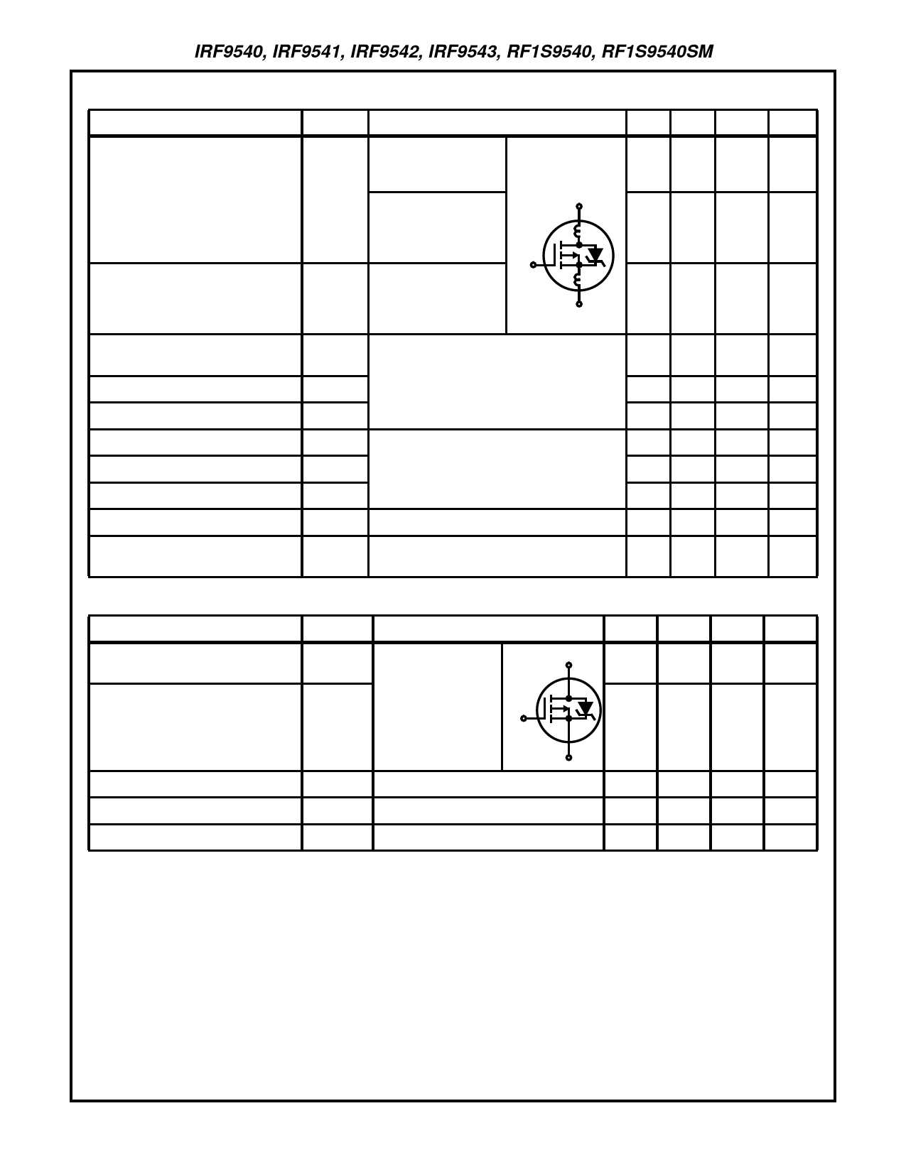
Modified MOSFET
-
Contact Screw on Tab Symbol Showing the
to the Center of Die
Internal Devices
Inductances
Measured From the
D
-
Drain Lead, 6mm
(0.25in) from Package
LD
to the Center of Die
G
LS
Measured From the
Source Lead, 6mm
(0.25in) From Package
LS
-
S
to Source Bonding Pad
Total Gate Charge
(Gate to Source + Gate to Drain)
Gate to Source Charge
Gate to Drain “Miller” Charge
Qg(TOT) VGS = -10V, ID = -19A, VDS = 80V Max,
-
Ig(REF) = -1.5mA
(See Figure 20 for Test Circuit) Gate Charge
Qgs is Essentially Independent of Operating
-
Temperature
Qgd
-
Input Capacitance
Output Capacitance
CISS VDS = -25V, VGS = 0V, f = 1MHz
-
(Figure 11)
COSS
-
Reverse Transfer Capacitance
CRSS
-
Thermal Resistance Junction to Case
RθJC
-
Thermal Resistance
RθJA Typical Socket Mount
-
Junction to Ambient
TYP
3.5
4.5
7.5
70
14
56
1100
550
250
-
-
MAX
-
UNITS
nH
-
nH
-
nH
90
nC
-
nC
-
nC
-
pF
-
pF
-
pF
1
oC/W
80
oC/W
Source to Drain Diode Specifications
PARAMETERS
Continuous Source Current
(Body Diode)
Pulse Source Current
(Body Diode)
(Note 3)
SYMBOL
TEST CONDITIONS
MIN
TYP MAX UNITS
ISD
Modified MOSFET
Symbol Showing the
Integral Reverse
ISM
P-N Junction Diode
G
-
D
-
-
-19
A
-
-76
A
S
Source to Drain Diode Voltage (Note 2)
VSD
TC = 25oC, ISD = -19A, VGS = 0V
-
Reverse Recovery Time
trr
TJ = 150oC, ISD = 19A, dISD/dt = 100A/µs
-
Reverse Recovery Charge
QRR
TJ = 150oC, ISD = 19A, dISD/dt = 100A/µs
-
-
-1.5
V
170
-
ns
0.8
-
µC
NOTES:
1. TJ = 25oC to TJ = 175oC.
2. Pulse test: pulse width ≤ 300µs, duty cycle ≤ 2%.
3. Repetitive rating: pulse width limited by maximum junction temperature. See Transient Thermal Impedance curve (Figure 3).
4. VDD = 25V, starting TJ = 25oC, L = 4mH, RG = 25Ω, peak IAS = 19A. (Figures 15, 16).
3
Share Link: 