RF2172PCBA410 Просмотр технического описания (PDF) - RF Micro Devices
Номер в каталоге
Компоненты Описание
производитель
RF2172PCBA410 Datasheet PDF : 14 Pages
| |||
RF2172
Pin Function Description
Interface Schematic
1
GND
Ground connection. For best performance, keep traces physically short
and connect immediately to the ground plane.
2
GND
Ground connection for the driver stage. For best performance, keep
traces physically short and connect immediately to the ground plane.
3
RF IN
RF input. This is a 50Ω input. No external matching is needed. An
See pin 15.
external DC blocking capacitor is required if this port is connected to a
DC path to ground or a DC voltage.
4
GND
See pin 1.
5
GND
See pin 1.
6
VPD
Power down pin. When this pin is 0V, the device will be in power down
mode, dissipating minimum DC power. This pin also serves as the VCC
supply pin for the bias circuitry. VPD should be at the supply voltage
when the part is not in power down mode.
7
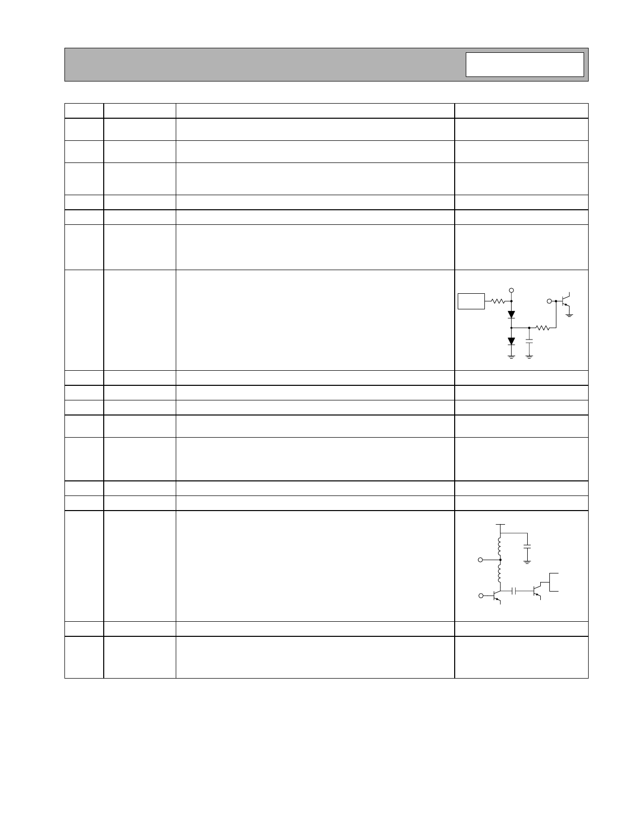
APC
Analog power control. Output power varies as a function of the voltage
on this pin. See graph. This pin must be driven through a series resistor
APC
with a voltage between 0V and VCC. Series resistor determines
dynamic range of power control. See plot “POUT versus Gain Control
Bias
Network
RF IN
versus Gain Control Resistor”.
1st
Stage
8
9
10
11
12
13
14
15
16
Pkg
Base
GND
GND
GND
RF OUT
RF OUT
GND
GND
VCC
GND
GND
See pin 1.
See pin 1.
See pin 1.
RF output. An external matching network is required to provide the opti-
mum load impedance at this pin.
RF output and power supply for the output stage. Bias voltage for the
output stage is provided through this pin. A shunt cap resonating with
the bond wire inductance at 2xf0 can also be used at this pin to provide
a second harmonic trap.
See pin 1.
See pin 15.
See pin 15.
See pin 1.
Power supply for driver stage and interstage matching. This pin forms
the shunt inductance needed for proper tuning of the interstage. Refer
to the application schematic for the proper configuration. Note: Position
and value of the components are important.
VCC
Inductor
Pin 15
Bond
Wire
External Cap
GND
RF OUT
RF IN
1st Stage
RF OUT
2nd Stage
See pin 1.
Ground connection for the output stage. This pad should be connected
to the groundplane by vias directly under the device. A short path is
required to obtain optimum performance, as well as provide a good
thermal path to the PCB for maximum heat dissipation.
Rev A11 030729
2-3
Share Link: 