RF2369 Просмотр технического описания (PDF) - RF Micro Devices
Номер в каталоге
Компоненты Описание
производитель
RF2369 Datasheet PDF : 10 Pages
| |||
RF2369
Preliminary
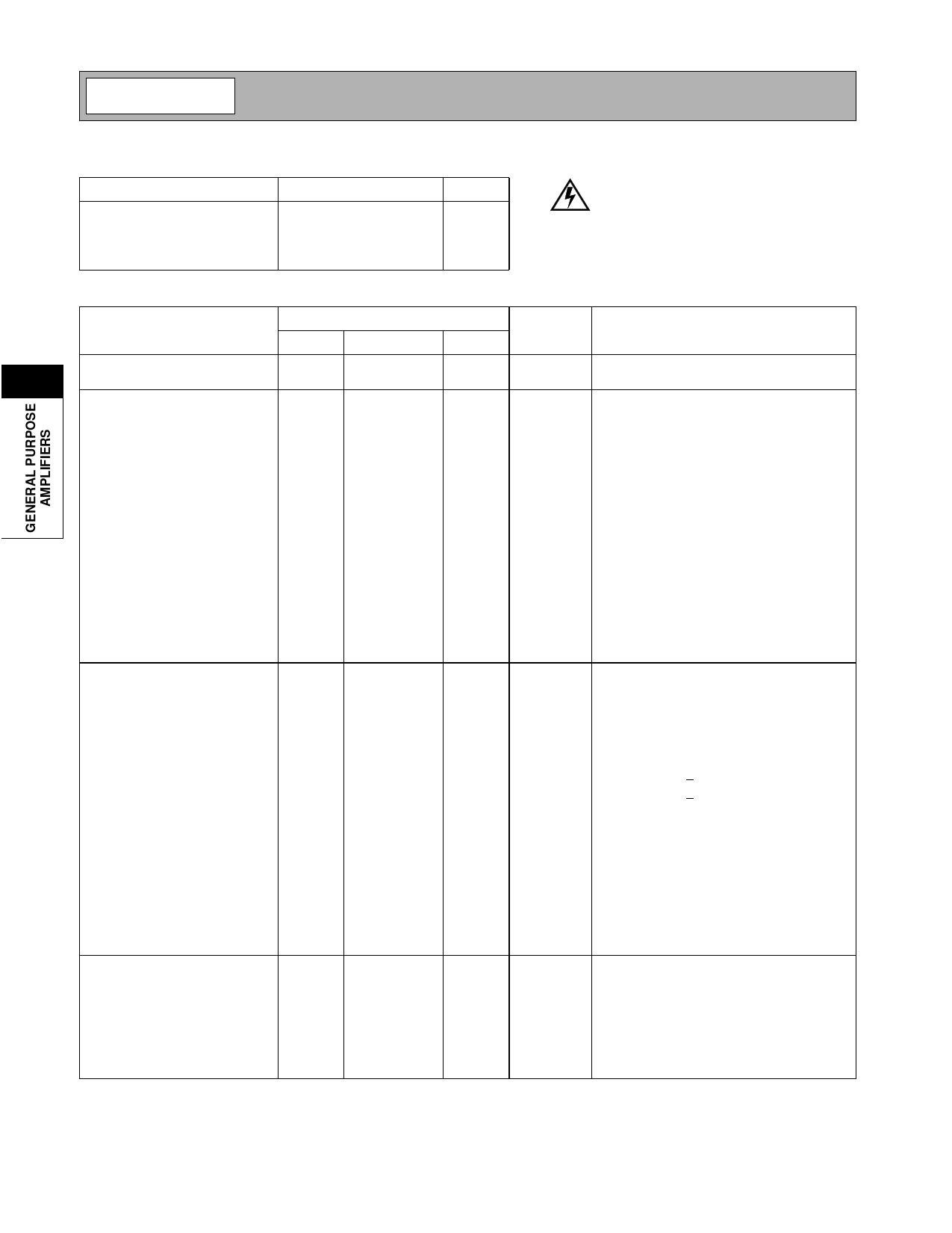
Absolute Maximum Ratings
Parameter
Supply Voltage
Input RF Level
Operating Ambient Temperature
Storage Temperature
Rating
-0.5 to +8.0
+10
-40 to +85
-40 to +150
Unit
VDC
dBm
°C
°C
Caution! ESD sensitive device.
RF Micro Devices believes the furnished information is correct and accurate
at the time of this printing. However, RF Micro Devices reserves the right to
make changes to its products without notice. RF Micro Devices does not
assume responsibility for the use of the described product(s).
Parameter
Overall
4
Frequency Range
Cellular Low Noise
Amplifier
Frequency
HIGH GAIN MODE
Gain
Noise Figure
Input IP3
Input VSWR
Output VSWR
Current Drain
BYPASS MODE
Gain
Input IP3
Input VSWR
Output VSWR
Current Drain
Cellular CDMA Driver
Frequency
HIGH GAIN MODE
Gain
Noise Figure
Output Power
ACPR1
ACPR2
Input VSWR
Output VSWR
Current Drain
BYPASS MODE
Gain
Input IP3
Input VSWR
Output VSWR
Current Drain
Power Supply
Voltage (VCC)
VSELECT Low
VSELECT High
Power Down
Specification
Min.
Typ.
Max.
150
824 to 894
2500
Unit
MHz
Condition
TAMB=25°C, VCC=3.0V
869
14.0
9.0
-3
+10
824
14.0
4
-3.0
+10
1.8
0
15.5
1.6
11.5
7.5
-2
+24
2.0
15.5
2.0
-65
-70
8.5
-2.0
+24
2.0
3
894
17.0
2.0
2:1
2:1
10.0
-1
2:1
2:1
4.0
849
17.0
2.5
2:1
2:1
-1.0
2:1
2:1
4.0
0.8
10
MHz
dB
dB
dBm
Gain Select<0.8V, VPD/VREF=3V
mA
dB
dBm
Gain Select>1.8V, VPD/VREF=0V
mA
MHz
dB
dB
dBm
dBc/30 kHz
dBc/30 kHz
Gain Select<0.8V, VPD/VREF=3V
POUT=+4dBm, +885kHz offset
POUT=+4dBm, +1.98MHz offset
mA
dB
dBm
Gain Select>1.8V, VPD/VREF=0V
mA
V
V
High Gain mode.
Select<0.8V, VPD/VREF=3V
V
Low Gain mode.
Select>1.8V, VPD/VREF=0V
µA
Gain Select<0.8V, VPD/VREF=0V, VCC=0V
4-184
Rev A3 010720
Share Link: 