HI5762/6IN Просмотр технического описания (PDF) - Renesas Electronics
Номер в каталоге
Компоненты Описание
производитель
HI5762/6IN Datasheet PDF : 16 Pages
| |||
HI5762
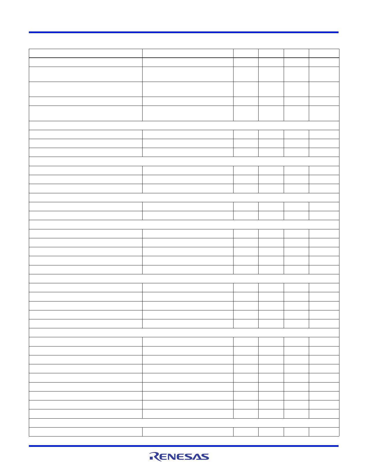
Electrical Specifications AVCC1,2 = DVCC1,2 = +5.0V, DVCC3 = +3.0V; VRIN = 2.50V; fS = 60MSPS at 50% Duty Cycle;
CL = 10pF; TA = +25°C; Differential Analog Input; Unless Otherwise Specified (Continued)
PARAMETER
TEST CONDITIONS
MIN
TYP
MAX
Analog Input Capacitance, CIN+ or CIN-
Analog Input Bias Current, IB+ or IB-
VIN+, VIN- = 2.5V, DC
VIN+, VIN- = VREF-, VREF+,DC
(Note 4, 5)
-
10
-
-10
-
10
Differential Analog Input Bias Current
IBDIFF = (IB+ - IB-)
Full Power Input Bandwidth, FPBW
(Notes 4, 5)
(Note 4)
-0.5
-
+0.5
-
250
-
Analog Input Common Mode Voltage Range
(VIN+ + VIN-)/2
INTERNAL VOLTAGE REFERENCE
Differential Mode (Note 4)
0.25
-
4.75
Reference Output Voltage, VROUT (Loaded)
Reference Output Current, IROUT
Reference Temperature Coefficient
2.35
2.5
2.65
-
2
4
-
-400
-
REFERENCE VOLTAGE INPUT
Reference Voltage Input, VRIN
Total Reference Resistance, RRIN
Reference Current, IRIN
DC BIAS VOLTAGE
with VRIN = 2.5V
with VRIN = 2.5V
-
2.5
-
-
1.25
-
-
2
-
DC Bias Voltage Output, VDC
Maximum Output Current
-
3.0
-
-
-
0.4
SAMPLING CLOCK INPUT
Input Logic High Voltage, VIH
Input Logic Low Voltage, VIL
Input Logic High Current, IIH
Input Logic Low Current, IIL
Input Capacitance, CIN
DIGITAL OUTPUTS
CLK
CLK
CLK, VIH = 5V
CLK, VIL = 0V
CLK
2.0
-
-
-
-
0.8
-10.0
-
+10.0
-10.0
-
+10.0
-
7
-
Output Logic High Voltage, VOH
Output Logic Low Voltage, VOL
Output Logic High Voltage, VOH
Output Logic Low Voltage, VOL
Output Capacitance, COUT
TIMING CHARACTERISTICS
IOH = 100µA; DVCC3 = 5V
IOL = 100µA; DVCC3 = 5V
IOH = 100µA; DVCC3 = 3V
IOL = 100µA; DVCC3 = 3V
4.0
-
-
-
-
0.8
2.4
-
-
-
-
0.5
-
7
-
Aperture Delay, tAP
Aperture Jitter, tAJ
Data Output Hold, tH
Data Output Delay, tOD
Data Latency, tLAT
Power-Up Initialization
For a Valid Sample (Note 4)
Data Invalid Time (Note 4)
-
5
-
-
5
-
-
10.7
-
-
11.7
-
6
6
6
-
-
20
Sample Clock Pulse Width (Low)
(Note 4)
7.5
8.3
-
Sample Clock Pulse Width (High)
(Note 4)
7.5
8.3
-
Sample Clock Duty Cycle Variation
-
5
-
POWER SUPPLY CHARACTERISTICS
Analog Supply Voltage, AVCC
(Note 4)
4.75
5.0
5.25
UNITS
pF
µA
µA
MHz
V
V
mA
ppm/oC
V
k
mA
V
mA
V
V
µA
µA
pF
V
V
V
V
pF
ns
psRMS
ns
ns
Cycles
Cycles
ns
ns
%
V
FN4318 Rev 3.00
January 22, 2010
Page 7 of 16
Share Link: 