HI5762/6IN Просмотр технического описания (PDF) - Renesas Electronics
Номер в каталоге
Компоненты Описание
производитель
HI5762/6IN Datasheet PDF : 16 Pages
| |||
HI5762
Absolute Maximum Ratings TA = +25°C
Supply Voltage, AVCC or DVCC to AGND or DGND . . . . . . . . . . .6V
DGND to AGND . . . . . . . . . . . . . . . . . . . . . . . . . . . . . . . . . . . . . 0.3V
Digital I/O Pins . . . . . . . . . . . . . . . . . . . . . . . . . . . . . DGND to DVCC
Analog I/O Pins . . . . . . . . . . . . . . . . . . . . . . . . . . . . AGND to AVCC
Operating Conditions
Temperature Range . . . . . . . . . . . . . . . . . . . . . . . . . .-40°C to +85°C
Thermal Information
Thermal Resistance (Typical, Note 3)
JA (°C/W)
44 Ld MQFP Package . . . . . . . . . . . . . . . . . . . . . . .
75
Maximum Junction Temperature . . . . . . . . . . . . . . . . . . . . . . +150°C
Maximum Storage Temperature Range . . . . . . . . . -65°C to +150°C
Pb-Free Reflow Profile. . . . . . . . . . . . . . . . . . . . . . . . .see link below
http://www.intersil.com/pbfree/Pb-FreeReflow.asp
CAUTION: Do not operate at or near the maximum ratings listed for extended periods of time. Exposure to such conditions may adversely impact product reliability and
result in failures not covered by warranty.
NOTE:
3. JA is measured with the component mounted on a high effective thermal conductivity test board in free air. See Tech Brief TB379 for details.
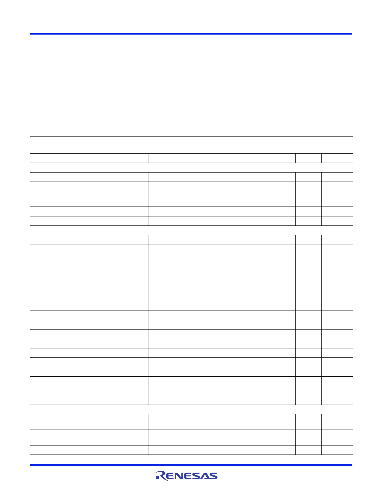
Electrical Specifications AVCC1,2 = DVCC1,2 = +5.0V, DVCC3 = +3.0V; VRIN = 2.50V; fS = 60MSPS at 50% Duty Cycle;
CL = 10pF; TA = +25°C; Differential Analog Input; Unless Otherwise Specified
PARAMETER
TEST CONDITIONS
MIN
TYP
MAX
ACCURACY
Resolution
10
-
-
Integral Linearity Error, INL
Differential Linearity Error, DNL
(Guaranteed No Missing Codes)
fIN = 10MHz
fIN = 10MHz
-
±2
-
-
±0.4
±1.0
Offset Error, VOS
Full Scale Error, FSE
DYNAMIC CHARACTERISTICS
fIN = DC
fIN = DC
-40
-
+40
-
4
-
Minimum Conversion Rate
No Missing Codes
-
1
-
Maximum Conversion Rate
No Missing Codes
60
-
-
Effective Number of Bits, ENOB
Signal to Noise and Distortion Ratio, SINAD
= R-----M-----S------NR----oM---i--sS---e---S--+--i-g--D--n--i-as---lt--o---r--t--i-o----n-
fIN = 10MHz
fIN = 10MHz
8.4
8.8
-
-
54.7
-
Signal to Noise Ratio, SNR
= R-R----M-M----S-S-----SN----i-og---in-s---ae---l
fIN = 10MHz
-
54.7
-
Total Harmonic Distortion, THD
2nd Harmonic Distortion
3rd Harmonic Distortion
Spurious Free Dynamic Range, SFDR
Intermodulation Distortion, IMD
I/Q Channel Crosstalk
I/Q Channel Offset Match
I/Q Channel Full Scale Error Match
Transient Response
Overvoltage Recovery
ANALOG INPUT
Maximum Peak-to-Peak Differential Analog Input
Range (VIN+ - VIN-)
Maximum Peak-to-Peak Single-Ended
Analog Input Range
Analog Input Resistance, RIN+ or RIN-
fIN = 10MHz
fIN = 10MHz
fIN = 10MHz
fIN = 10MHz
f1 = 1MHz, f2 = 1.02MHz
(Note 4)
0.2V Overdrive (Note 4)
VIN+, VIN- = VREF, DC
-
-68
-
-
-70
-
-
-73
-
-
70
-
-
64
-
-
-75
-
-
10
-
-
10
-
-
1
-
-
1
-
-
0.5
-
-
1.0
-
-
1
-
UNITS
Bits
LSB
LSB
LSB
LSB
MSPS
MSPS
Bits
dB
dB
dBc
dBc
dBc
dBc
dBc
dBc
LSB
LSB
Cycle
Cycle
V
V
M
FN4318 Rev 3.00
January 22, 2010
Page 6 of 16
Share Link: 