HA5351 Просмотр технического описания (PDF) - Renesas Electronics
Номер в каталоге
Компоненты Описание
производитель
HA5351 Datasheet PDF : 7 Pages
| |||
HA5351
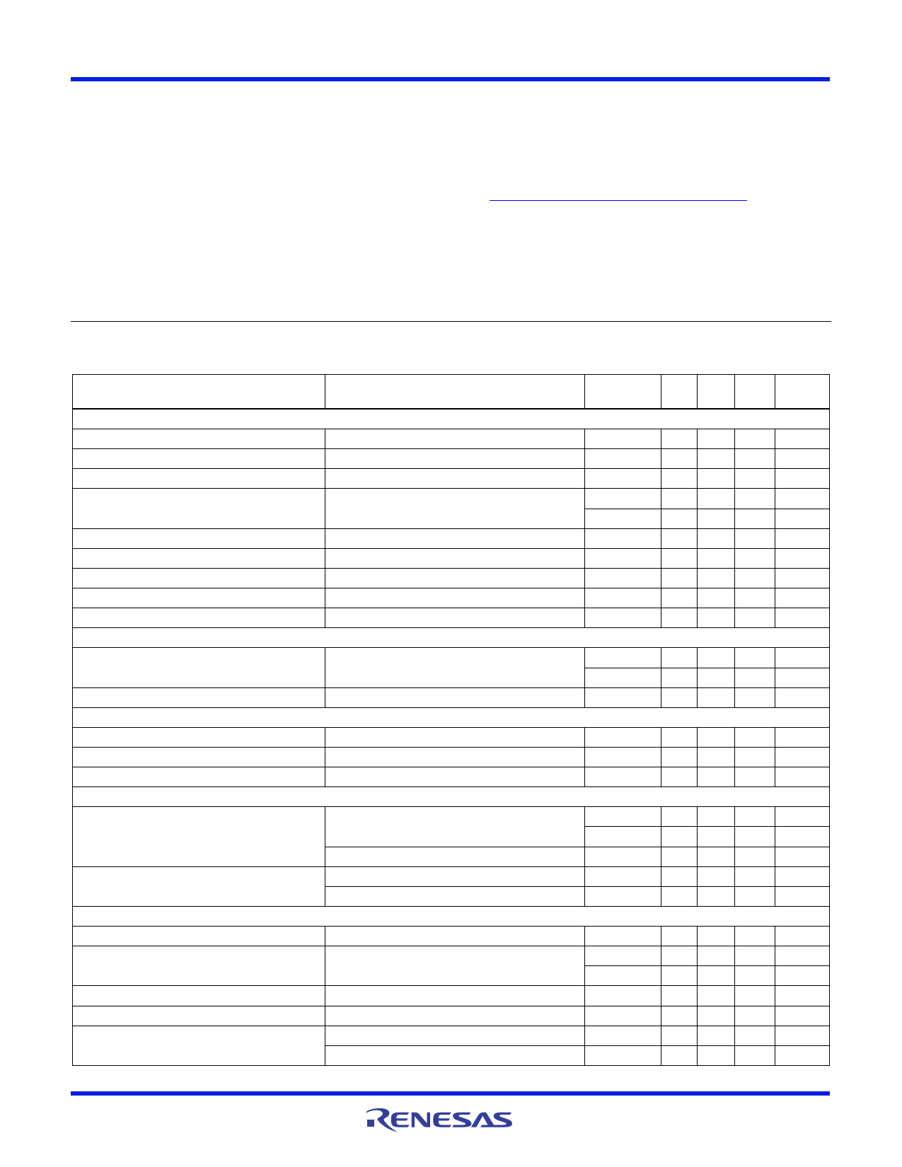
Absolute Maximum Ratings
Voltage Between V+ and V- Terminals. . . . . . . . . . . . . . . . . . . .+11V
Differential Input Voltage . . . . . . . . . . . . . . . . . . . . . . . . . . . . . . . 6V
Voltage Between Sample and Hold Control and Ground. . . . . +5.5V
Output Current, Continuous . . . . . . . . . . . . . . . . . . . . . . . . . . 37mA
Operating Conditions
Temperature Range . . . . . . . . . . . . . . . . . . . . . . . . . .-40°C to +85°C
Thermal Information
Thermal Resistance (Typical, Note 1)
JA (°C/W)
SOIC Package . . . . . . . . . . . . . . . . . . . . . . . . . . . . .
160
Maximum Junction Temperature (Plastic Package) . . . . . . . +150°C
Maximum Storage Temperature Range . . . . . . . . . -65°C to +150°C
Pb-Free Reflow Profilesee link below
http://www.intersil.com/pbfree/Pb-FreeReflow.asp
CAUTION: Stresses above those listed in “Absolute Maximum Ratings” may cause permanent damage to the device. This is a stress only rating and operation of the
device at these or any other conditions above those indicated in the operational sections of this specification is not implied.
NOTE:
1. JA is measured with the component mounted on an evaluation PC board in free air.
Electrical Specifications
Test Conditions: VSUPPLY =5V; CH = Internal = 15pF, Digital Input: VIL = 0V (Sample), VIH = 4.0V (Hold).
Non-Inverting Unity Gain Configuration (Output Tied to -Input), CL = 5pF,
Unless Otherwise Specified
PARAMETER
TEST CONDITIONS
TEMP.
(°C)
MIN TYP MAX UNITS
INPUT CHARACTERISTICS
Input Voltage Range
Full
-2.5 - +2.5
V
Input Resistance (Note 2)
+25
100 500 -
k
Input Capacitance
+25
-
-
5
pF
Input Offset Voltage
+25
-2
-
2
mV
Full
-3.0 -
3.0
mV
Offset Voltage Temperature Coefficient
Full
- 15
-
µV/°C
Bias Current
Full
- 2.5 5
µA
Offset Current
Full
-1.5 - +1.5 µA
Common Mode Range
Full
-2.5 - +2.5
V
Common Mode Rejection Ratio
2.5V, Note 3
Full
60 80
-
dB
TRANSFER CHARACTERISTICS
Large Signal Voltage Gain
VOUT = 2.5V
+25
95 108 -
dB
Full
85 -
-
dB
Unity Gain -3dB Bandwidth
25
- 40
-
MHz
TRANSIENT RESPONSE
Rise Time
200mV Step
+25
- 8.5 -
ns
Overshoot
200mV Step
+25
0
-
30
%
Slew Rate
5V Step
Full
88 105 -
V/µs
DIGITAL INPUT CHARACTERISTICS
Input Voltage
VIH
+25, +85 2.1 -
5.0
V
-40
2.4 -
5.0
V
Input Current
OUTPUT CHARACTERISTICS
VIL
VIL = 0V
VIH = 5V
Full
0
-
0.8
V
Full
-1.0 -
1.0
µA
Full
-1.0 -
1.0
µA
Output Voltage
Output Current
RL = 510
RL = 100
Full
-3.0 - +3.0
V
+25, +85 20 25
-
mA
-40
15 -
-
mA
Full Power Bandwidth
Output Resistance
5VP-P, AV = +1, -3dB
Hold Mode
Full
- 13
-
MHz
+25
- 0.02 -
Total Output Noise
(DC to 10MHz)
Sample Mode
Hold Mode
+25
- 325
-
µVRMS
+25
- 325
-
µVRMS
FN3690 Rev 11.00
April 25, 2013
Page 2 of 7
Share Link: 