KSC5367F Просмотр технического описания (PDF) - Fairchild Semiconductor
Номер в каталоге
Компоненты Описание
производитель
KSC5367F Datasheet PDF : 6 Pages
| |||
KSC5367F
High Voltage and High Reliability
• High speed Switching
• Wide Safe Operating Area
• High Collector-Base Voltage
1
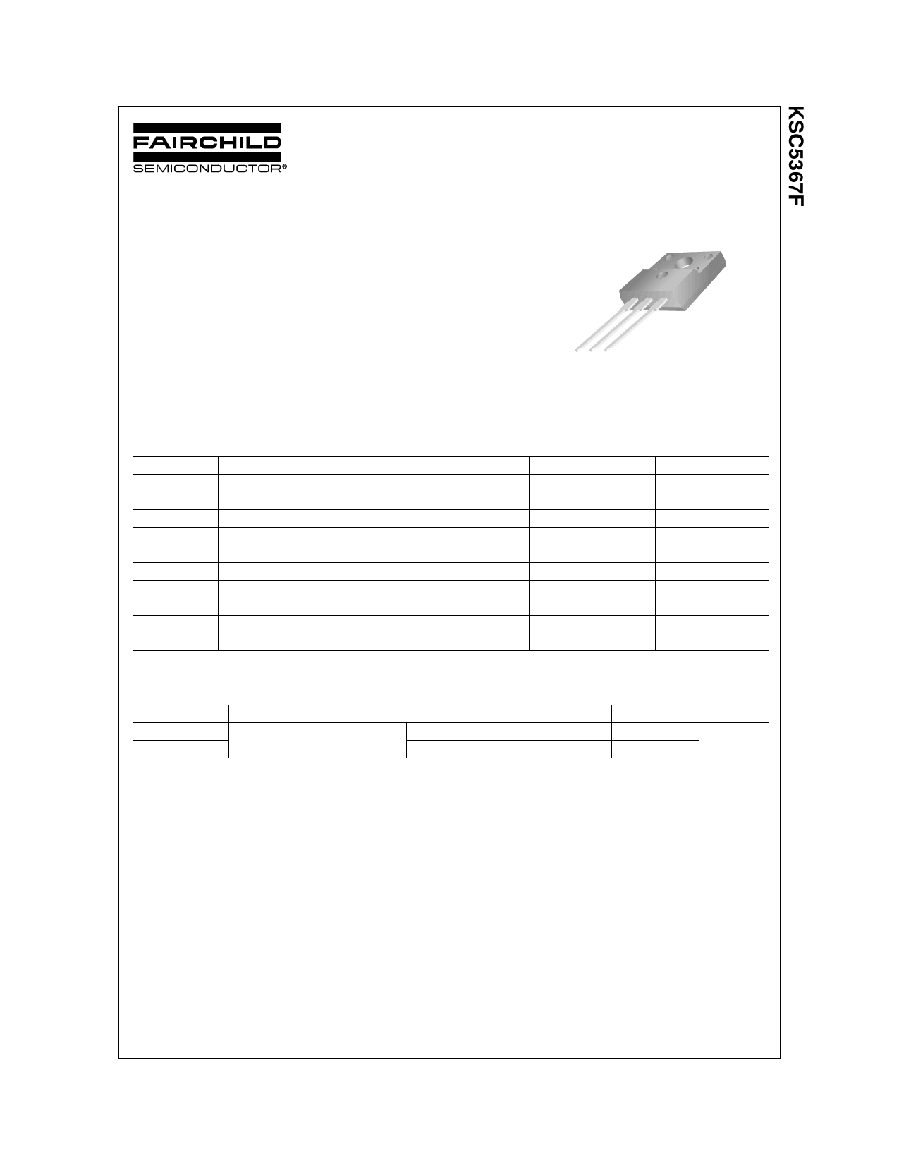
TO-220F
1.Base 2.Collector 3.Emitter
NPN Triple Diffused Planar Silicon Transistor
Absolute Maximum Ratings TC=25°C unless otherwise noted
Symbol
Parameter
VCBO
Collector-Base Voltage
VCEO
Collector-Emitter Voltage
VEBO
Emitter-Base Voltage
IC
Collector Current (DC)
ICP
*Collector Curren (Pulse)
IB
Base Current (DC)
IBP
*Base Current (Pulse)
PC
Power Dissipation(TC=25°C)
TJ
Junction Temperature
TSTG
Storage Temperature
* Pulse Test: Pulse Width=5ms, Duty Cycle≤10%
Value
1600
800
12
3
6
2
4
40
150
- 65 ~ 150
Units
V
V
V
A
A
A
A
W
°C
°C
Thermal Characteristics TC=25°C unless otherwise noted
Symbol
Characteristics
Rθjc
Thermal Resistance
Junction to Case
Rθja
Junction to Ambient
Rating
3.1
62.5
Unit
°C/W
©2002 Fairchild Semiconductor Corporation
Rev. B1, December 2002
Share Link: 