ADM208ARSZ Просмотр технического описания (PDF) - Analog Devices
Номер в каталоге
Компоненты Описание
производитель
ADM208ARSZ Datasheet PDF : 16 Pages
| |||
ADM206/ADM207/ADM208/ADM211/ADM213
GENERAL INFORMATION
The ADM2xx family of RS-232 drivers/ receivers is designed to
solve interface problems by meeting the EIA-232-E
specifications while using a single digital 5 V supply. The EIA-
232-E standard requires transmitters that will deliver ±5 V
minimum on the transmission channel and receivers that can
accept signal levels down to ±3 V. The ADM2xx meet these
requirements by integrating step-up voltage converters and level
shifting transmitters and receivers onto the same chip. CMOS
technology is used to keep the power dissipation to an absolute
minimum. A comprehensive range of transmitter/ receiver
combinations is available to cover most communication needs.
The ADM2xx are modifications, enhancements, and
improvements to the AD2xx family and derivatives thereof. They
are essentially plug-in compatible and do not have materially
different applications.
The ADM206, ADM211, and ADM213 are particularly useful in
battery-powered systems because they feature a low power shut-
down mode that reduces power dissipation to less than 5 μW.
To facilitate sharing a common line or for connection to a
microprocessor data bus, the ADM206, the ADM211, and the
ADM213 feature an enable (EN) function. When the receivers
are disabled, their outputs are placed in a high impedance state.
CIRCUIT DESCRIPTION
The internal circuitry in the ADM2xx consists of three main
sections: (a) a charge pump voltage converter; (b) RS-232-to-
TTL/CMOS receivers; and (c) TTL/CMOS-to-RS-232
transmitters.
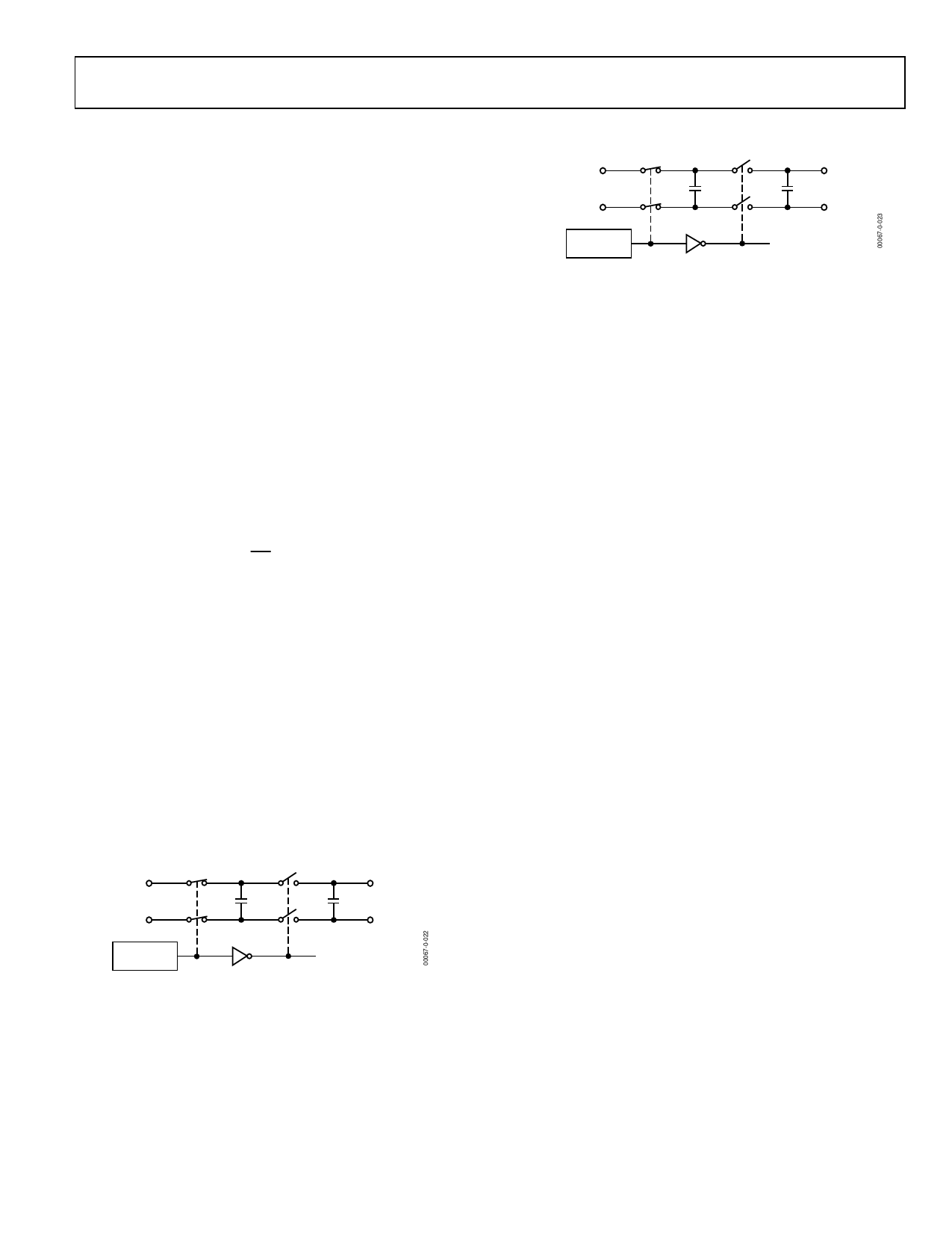
Charge Pump DC-to-DC Voltage Converter
The charge pump voltage converter consists of an oscillator and
a switching matrix. The converter generates a ±10 V supply
from the 5 V input. This is done in two stages using a switched
capacitor technique, as illustrated in Figure 20 and Figure 21.
First, the 5 V input supply is doubled to 10 V using capacitor C1
as the charge storage element. The 10 V level is then inverted to
generate –10 V using C2 as the storage element.
VCC
GND
S1
S3
+
C1
S2
S4
+
C3
V+ = 2VCC
VCC
INTERNAL
OSCILLATOR
Figure 20. Charge Pump Voltage Doubler
FROM V+
VOLTAGE
DOUBLER
GND
S1
S3
+
C2
S2
S4
+
C4
GND
V– = –(V+)
INTERNAL
OSCILLATOR
Figure 21. Charge Pump Voltage Inverter
Capacitors C3 and C4 are used to reduce the output ripple.
Their values are not critical and can be reduced if higher levels
of ripple are acceptable. The charge pump capacitors C1 and C2
may also be reduced at the expense of higher output impedance
on the V+ and V– supplies.
The V+ and V– supplies may also be used to power external
circuitry if the current requirements are small.
Transmitters (Drivers)
The drivers convert TTL/CMOS input levels into EIA-232-E
output levels. With VCC = +5 V and driving a typical EIA-232-E
load, the output voltage swing is ±9 V. Even under worst-case
conditions, the drivers are guaranteed to meet the ±5 V EIA-
232-E minimum requirement.
The input threshold levels are both TTL- and CMOS-compatible
with the switching threshold set at VCC/4. With a nominal VCC =
5 V, the switching threshold is 1.25 V typical. Unused inputs
may be left unconnected, because an internal 400 kΩ pull-up
resistor pulls them high, forcing the outputs into a low state.
As required by the EIA-232-E standard, the slew rate is limited
to less than 30 V/μs, without the need for an external slew
limiting capacitor, and the output impedance in the power-off
state is greater than 300 Ω.
Receivers
The receivers are inverting level shifters that accept EIA-232-E
input levels (±5 V to ±15 V) and translate them into 5 V TTL/
CMOS levels. The inputs have internal 5 kΩ pull-down resistors
to ground and are also protected against overvoltages of up to
±30 V. The guaranteed switching thresholds are 0.8 V minimum
and 2.4 V maximum, well within the ±3 V EIA-232-E require-
ment. The low level threshold is deliberately positive, since it
ensures that an unconnected input will be interpreted as a
low level.
The receivers have Schmitt-trigger inputs with a hysteresis level
of 0.65 V. This ensures error-free reception for both noisy
inputs and inputs with slow transition times.
Rev. D | Page 11 of 16
Share Link: 