CXD1171 Просмотр технического описания (PDF) - Harris Semiconductor
Номер в каталоге
Компоненты Описание
производитель
CXD1171 Datasheet PDF : 8 Pages
| |||
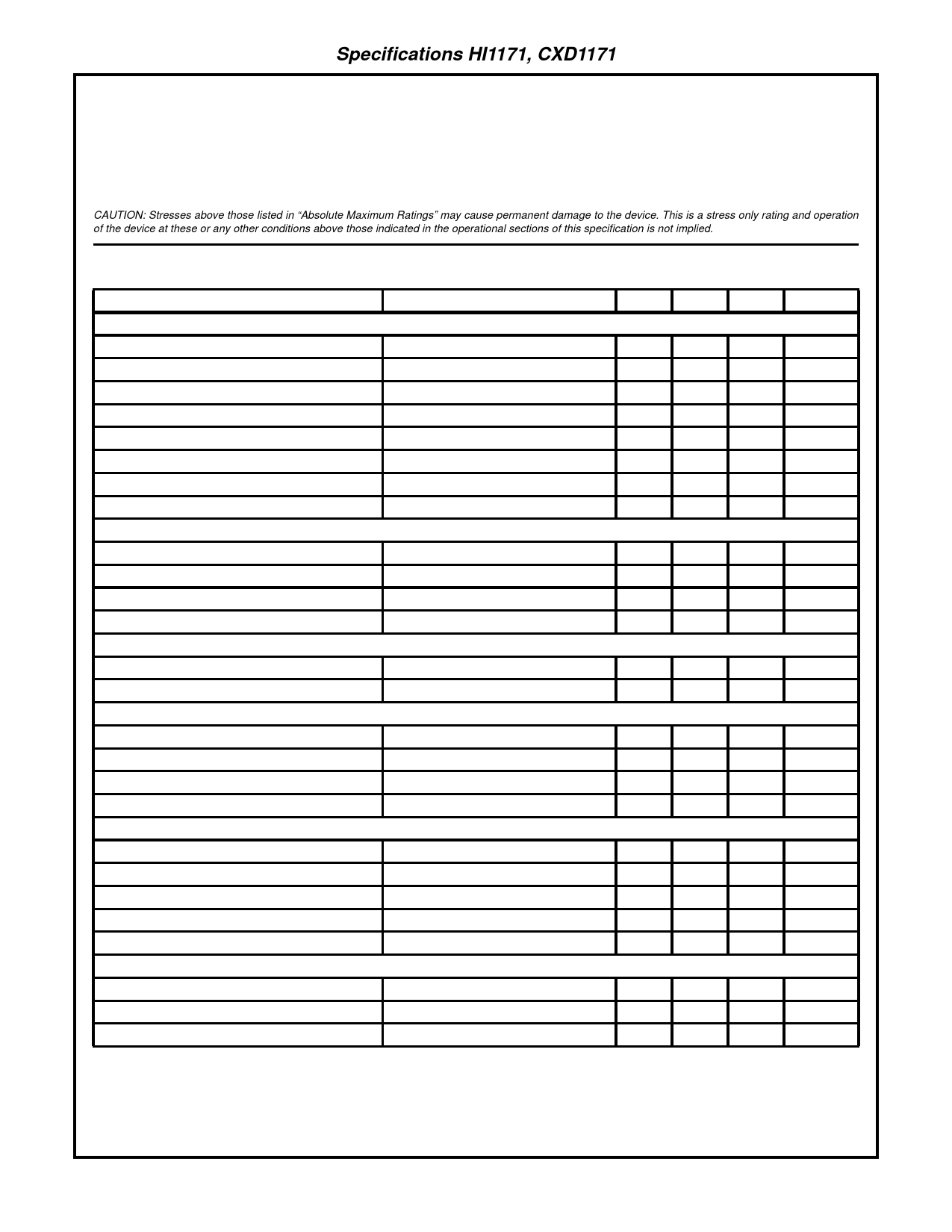
Specifications HI1171, CXD1171
Absolute Maximum Ratings
Thermal Information
Digital Supply Voltage DVDD to DVSS . . . . . . . . . . . . . . . . . . . +7.0V
Analog Supply Voltage AVDD to AVSS . . . . . . . . . . . . . . . . . . . +7.0V
Input Voltage. . . . . . . . . . . . . . . . . . . . . . . . . . . . . . . . . VDD to VSS V
Output Current . . . . . . . . . . . . . . . . . . . . . . . . . . . . . . .0mA to 15mA
Storage Temperature Range . . . . . . . . . . . . . . . . . -65oC to +150oC
Lead Temperature (Soldering 10s)(Lead Tips Only) . . . . . . +300oC
Thermal Resistance (Typ, Note 1)
θJA
SOIC Package. . . . . . . . . . . . . . . . . . . . . . . . . . . . . . . . . 98oC/W
Maximum Power Dissipation
HI1171JCB, CXD1171M . . . . . . . . . . . . . . . . . . . . . . . . . . 160mW
Operating Temperature Range . . . . . . . . . . . . . . . . . -20oC to +75oC
Junction Temperature . . . . . . . . . . . . . . . . . . . . . . . . . . . . . . +150oC
CAUTION: Stresses above those listed in “Absolute Maximum Ratings” may cause permanent damage to the device. This is a stress only rating and operation
of the device at these or any other conditions above those indicated in the operational sections of this specification is not implied.
Electrical Specifications AVDD = +4.75 to +5.25V, DVDD = +4.75 to +5.25V, VREF = +2.0V, fS = 40MHz,
CLK Pulse Width = 12.5ns, TA = +25oC (Note 4).
PARAMETER
TEST CONDITION
MIN
TYP
SYSTEM PERFORMANCE
Resolution
8
-
Integral Linearity Error, INL
Differential Linearity Error, DNL
Offset Error, VOS
Full Scale Error, FSE (Adjustable to Zero)
fS = 40MHz (End Point)
fS = 40MHz
(Note 2)
(Note 2)
-0.5
-
-
-
-
-
-
-
Full Scale Output Current, IFS
Full Scale Output Voltage, VFS
Output Voltage Range, VFSR
DYNAMIC CHARACTERISTICS
-
10
1.9
2.0
0.5
2.0
Throughput Rate
See Figure 7
40.0
-
Glitch Energy, GE
Differential Gain, ∆AV (Note 3)
Differential Phase, ∆φ (Note 3)
ROUT = 75Ω
-
30
-
1.2
-
0.5
REFERENCE INPUT
Voltage Reference Input Range
0.5
-
Reference Input Resistance
(Note 3)
1.0
-
DIGITAL INPUTS
Input Logic High Voltage, VIH
Input Logic Low Voltage, VIL
Input Logic Current, IIL, IIH
Digital Input Capacitance, CIN
TIMING CHARACTERISTICS
(Note 3)
(Note 3)
(Note 3)
(Note 3)
3.0
-
-
-
-
-
-
5.0
Data Setup Time, tSU
Data Hold Time, tHLD
Propagation Delay Time, tPD
Settling Time, tSET (to 1/2 LSB)
CLK Pulse Width, TPW1, TPW2
POWER SUPPLY CHARACTERISITICS
See Figure 1
See Figure 1
See Figure 9
See Figure 1
See Figure 1
5
-
10
-
-
10
-
10
12.5
-
IAVDD
14.3MHz, at Color Bar Data Input
-
10.9
IDVDD
14.3MHz, at Color Bar Data Input
-
4.2
Power Dissipation
200Ω load at 2VP-P Output
-
-
NOTES:
1. Dissipation rating assumes device is mounted with all leads soldered to printed circuit board
2. Excludes error due to external reference drift.
3. Parameter guaranteed by design or characterization and not production tested.
4. Electrical specifications guaranteed only under the stated operating conditions.
MAX
-
1.3
±0.25
0.125
±13
15
2.1
2.1
-
-
-
-
2.0
-
-
1.5
±5.0
-
-
-
-
15
-
11.5
4.8
80
UNITS
Bits
LSB
LSB
LSB
LSB
mA
V
V
MSPS
pV-s
%
Degree
V
MΩ
V
V
µA
pF
ns
ns
ns
ns
ns
mA
mA
mW
3
Share Link: 