MTL001 Просмотр технического описания (PDF) - Myson Century Inc
Номер в каталоге
Компоненты Описание
производитель
MTL001 Datasheet PDF : 64 Pages
| |||
MYSON
TECHNOLOGY
MTL001
(Rev. 0.95)
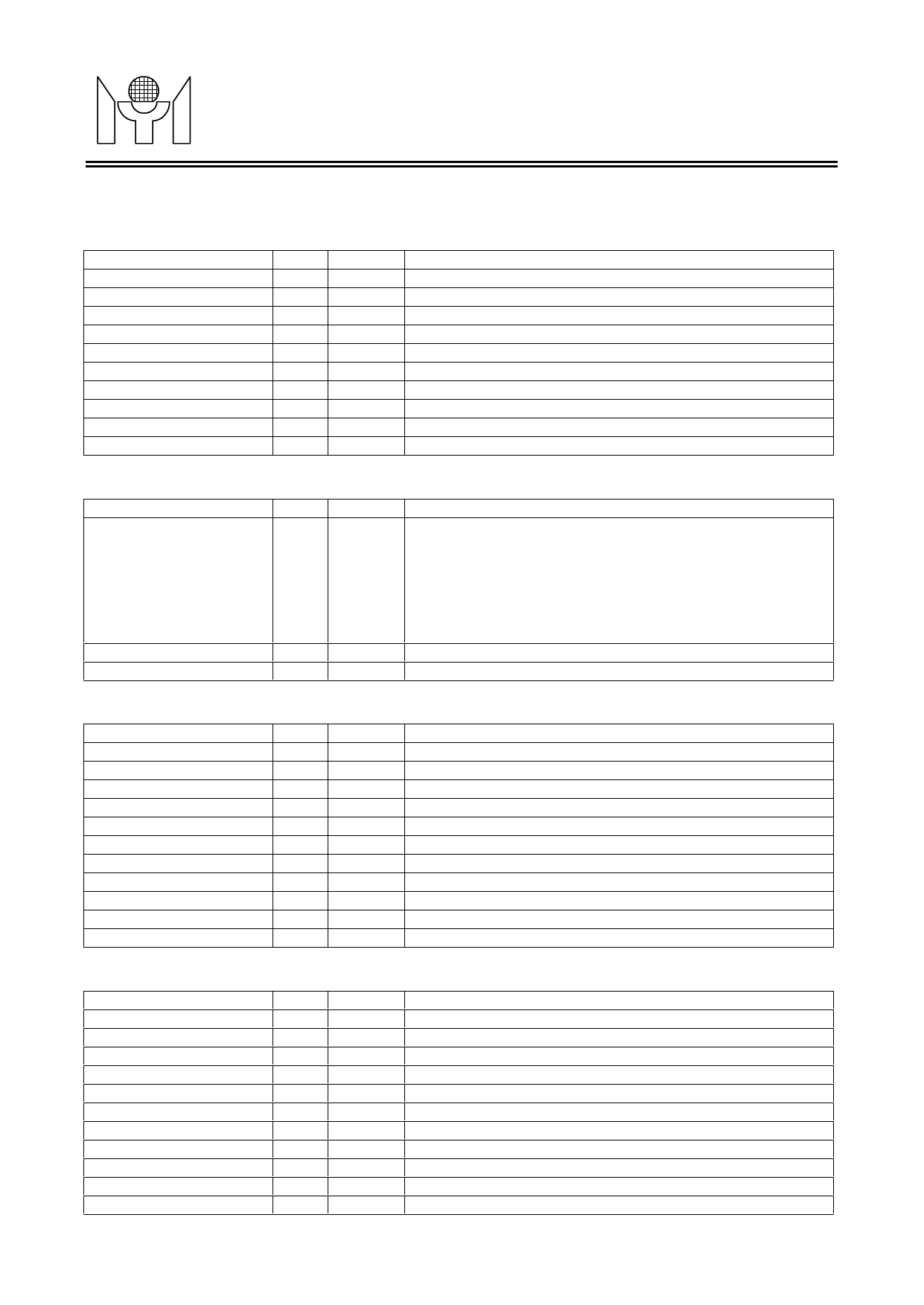
2. PIN DESCRIPTION
ADC1 Input Interface (YUV or RGB or TMDS Input Data)
Name
Type Pin# Description
VSYNC
I
249 Vertical sync input
HSYNC/CS
I
248 Horizontal or Composite sync input
RGBSEL
O
29 Input select. 1:RGB input, 0:YUV input
TMDSSEL
O
250 TMDS input select, active high
CLAMP
O
247 Clamp pulse output for ADC
IPCLK
I
253 Input pixel clock
R1IN[7:0]/YIN[7:0]
I
2-9 Red or Y channel or TMDS input data (Single/Dual ADC)
G1IN[7:0]/UVIN[7:0]
I
11-18 Green or UV channel or TMDS input data (Single/Dual ADC)
B1IN[7:0]
I
20-27 Blue channel or TMDS input data (Single/Dual ADC)
TDIE
I
251 TMDS digital input enable
ADC2 Input Interface (RGB Data)
Name
Type Pin#
R2IN[7:0]
I
31-38
G2IN[7:0]
B2IN[7:0]
I
40-47
I
49-56
Description
Red channel input data (Dual ADC)
or Control bit for YUV video input
Bit 4: VPHREF, Video input Horizontal reference signal
Bit 3: VPVS, Video input VSYNC signal
Bit 2: VPODD, Video input ODD/EVEN field signal
Bit 1: VPHS, Video input HSYNC signal
Bit 0: VPCLK, Video input clock signal
Green channel input data (Dual ADC)
Blue channel input data (Dual ADC)
Display Output Interface
Name
Type
DDEN
O
DVSYNC
O
DHSYNC
O
DDCLK1
O
DDCLK2
O
R1OUT[7:0]
O
G1OUT[7:0]
O
B1OUT[7:0]
O
R2OUT[7:0]
O
G2OUT[7:0]
O
B2OUT[7:0]
O
Pin#
124
123
122
94
93
113-120
104-111
96-103
84-91
75-82
67-74
Description
Display data output enable for LCD panel
Display Vertical sync output
Display Horizontal sync output
Display output clock for odd data
Display output clock for even data
Red output even data , bit[7:2] for 6-bit panel
Green output even data , bit[7:2] for 6-bit panel
Blue output even data , bit[7:2] for 6-bit panel
Red output odd data , bit[7:2] for 6-bit panel
Green output odd data , bit[7:2] for 6-bit panel
Blue output odd data , bit[7:2] for 6-bit panel
Memory Interface
Name
MCK
MCKE
MCS#
MRAS#
MCAS#
MWE#
DQM[1:0]
BA/MA11
DQM3/MA10
DQM2/MA9
MA[8:0]
Type
O
O
O
O
O
O
O
O
O
O
O
Pin#
180
178
168
197
196
195
198-199
182
149
148
183-191
Description
Memory output clock
Memory clock enable
Memory chip select, active low.
Memory row address strobe, active low
Memory column address strobe, active low
Memory write enable, active low
Memory data mask byte enable
Memory bank address or Memory address line
SGRAM data mask byte enable or SDRAM address line
SGRAM data mask byte enable or SDRAM address line
Memory address line
Revision 0.95
-4-
2000/06/14
Share Link: 