CXP402 Просмотр технического описания (PDF) - Sony Semiconductor
Номер в каталоге
Компоненты Описание
производитель
CXP402 Datasheet PDF : 16 Pages
| |||
CXP402
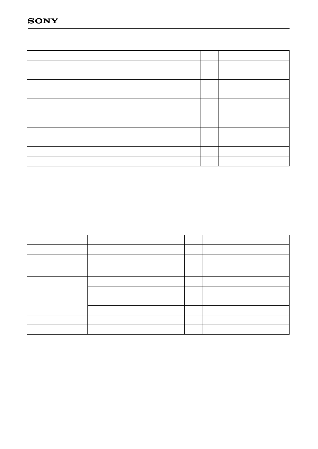
Absolute Maximum Ratings
(Vss = 0V reference)
Item
Supply voltage
LCD bias voltage
Input voltage
Output voltage
Symbol
Ratings
Unit
VDD
–0.3 to +7.0∗1
V
VLC1, VLC2, VLC3
–0.3 to +7.0∗2
V
VIN
–0.3 to +7.0∗2
V
VOUT
–0.3 to +7.0∗2
V
Remarks
High level output current
IOH
–5
mA Output pin (value per pin)
High level total output current ∑IOH
–70
mA Total of output pins
Low level output current
IOL
15
mA Output pin (value per pin)
Low level total output current ∑IOL
100
mA Total of output pins
Operating temperature
Topr
–20 to +75
°C
Storage temperature
Tstg
–40 to +125
°C
Allowable power dissipation PD
600
mW
∗1 The potential difference between analog power supplies AVDD, AVss, the oscillation power supplies XVDD,
XVss and VDD, Vss should be within ±0.3V.
∗2 VLC1, VLC2, VLC3, VIN and VOUT should not exceed VDD + 0.3V.
Note) Usage exceeding absolute maximum ratings may permanently impair the LSI. Normal operation should
be conducted under the recommended conditions. Exceeding those conditions may adversely affect the
reliability of the LSI.
Recommended Operation Conditions
(Vss = 0V reference)
Item
Symbol
Min.
Max.
Unit
Remarks
Supply voltage
VDD
3.4
5.25
V Operation guaranteed range
LCD bias voltage
VLC1,
VLC2,
VLC3
VSS
VDD
V
Liquid crystal power supply
range∗1
VIH
High level input voltage
VIHS
0.7VDD
0.8VDD
VDD
V
VDD
V Hysteresis input∗2
VIL
Low level input voltage
VILS
Analog input voltage VIA
0
0.3VDD
V
0
0.2VDD
V Hysteresis input∗2
0
VDD
V ∗3
Operating temperature Topr
–20
+75
°C
∗1 The optimal value depends on the characteristics of the used LCD element. Also, the LCD bias voltage is
biased to 1/3 the supply voltage by the resistor of approximately 20kΩ in the LSI.
∗2 RME, XRST, EXCK, FOK, SEIN, CNIN, VCKI, LRCKI, BCKI, PCMDI pins
∗3 CLTV, FILI, RF, VCTL, AIN1, AIN2, BAIS, ASYI pins
– 11 –
Share Link: 