MRFIC1818 Просмотр технического описания (PDF) - Motorola => Freescale
Номер в каталоге
Компоненты Описание
производитель
MRFIC1818 Datasheet PDF : 8 Pages
| |||
Typical Characteristics
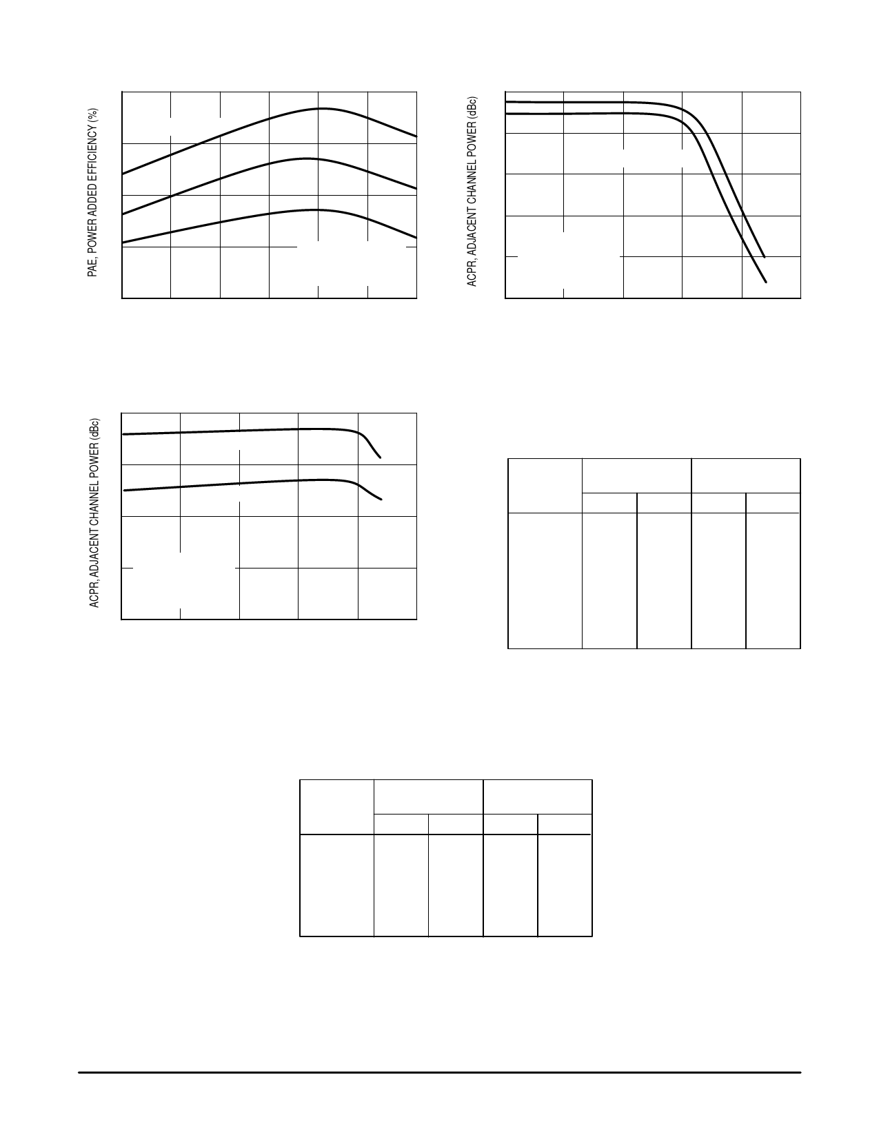
47
TA = –35°C
45
25°C
43
85°C
41
Pin = 3 dBm
VD1, VD2, VD3 = 4.8 V
VSS = –4 V
39
1.85
1.86
1.87
1.88
1.89
1.9
1.91
f, FREQUENCY (GHz)
Figure 15. Power Added Efficiency versus
Frequency – PCS Band
50
5.6 V
45
VD1, VD2, VD3 = 4.8 V
40
35
f = 1880 MHz
30 Carrier BW = 30 kHz
Channel BW = 30 kHz
Temp = 25°C
25
10
15
20
25
30
35
Pout, OUTPUT POWER (dBm)
Figure 16. CDMA ACPR at 885 kHz Offset versus
Output Power
50
VD1, VD2, VD3 = 5.6 V
49
4.8 V
48
47
f = 1880 MHz
Carrier BW = 30 kHz
Channel BW = 30 kHz
Temp = 25°C
46
10
15
20
25
30
35
Pout, OUTPUT POWER (dBm)
Figure 17. CDMA ACPR at 1980 kHz Offset
versus Output Power
Table 1. Optimum Loads Derived from
Circuit Characterization
Zin
ZOL*
f
OHMS
OHMS
MHz
R
jX
R
jX
1710
9.19
–30.10
6.00
3.80
1720
9.35
–29.60
5.96
3.71
1730
9.50
–29.30
5.88
3.60
1740
9.65
–29.10
5.80
3.46
1750
9.60
–29.00
5.75
3.33
1760
9.42
–28.79
5.67
3.20
1770
9.11
–28.60
5.60
3.07
1780
8.77
–28.30
5.51
2.93
1785
8.54
–28.15
5.45
2.79
Zin represents the input impedance of the device.
ZOL* represents the conjugate of the optimum output load to present
to the device.
Table 2. Optimum Loads Derived from
Circuit Characterization – PCS Board
Zin
ZOL*
OHMS
f
OHMS
MHz
R
jX
R
jX
1850
3.92
–43.30
7.70
0.39
1860
4.01
–43.56
7.64
0.23
1870
4.08
–43.78
7.57
0.15
1880
4.19
–44.00
7.51
0.07
1890
4.29
–44.29
7.50
–0.04
1900
4.31
–44.49
7.44
–0.06
1910
4.37
–44.81
7.35
–0.19
Zin represents the input impedance of the device.
ZOL* represents the conjugate of the optimum output load to present
to the device.
MRFIC1818
6
MOTOROLA RF DEVICE DATA
Share Link: 