PI74LCX16652A Просмотр технического описания (PDF) - Pericom Semiconductor
Номер в каталоге
Компоненты Описание
производитель
PI74LCX16652A Datasheet PDF : 7 Pages
| |||
PI74LCX16652
12345678901234567890123456789012123456789012345678901234567890121234567890123456789012345678901212314656-7B89i0t12R34e5g67i8s9t0e1r23e4d56T789r0a12n1s2c34e5i6v78e9r0s12
Truth Table(1)
Inputs
Data I/O(2)
Function/Operation
xOEAB xOEBA xCLKAB xCLKBA xSAB xSBA
xAx
xBx
Isolation
Store A and B Data
L
H
H or L
H or L
X
X
L
H
↑
↑
X
X
Input
Input
Store A, Hold B
Store A in Both Registers
X
H
H
H
↑
H or L
X
X
↑
↑
X(2)
X
Input
Input
Unspecified(1)
Output
Hold A, Store B
Store B in Both Registers
L
X
H or L
↑
L
L
↑
↑
X
X
Unspecified(1)
X
X(2)
Output
Input
Input
Real Time B Data to A Bus
Stored B Data to A Bus
L
L
X
X
X
L
L
L
X
H or L
X
H
Output
Input
Real Time A Data to B Bus
Stored A Data to B Bus
H
H
X
X
H
H
H or L
X
L
X
H
X
Input
Output
Stored A Data to B Bus and
Stored B Data to A Bus
H
L
H or L
H or L
H
H
Output
Output
Notes:
1. The data output functions may be enabled or disabled by various signals at the xOEAB or xOEBA inputs. Data
input functions are always enabled, i.e., data at the bus pins will be stored on every low-to-high transition
on the clock inputs.
2. Select control = L: clocks can occur simultaneously.
Select control = H: clocks must be staggered in order to load both registers.
H = High Voltage Level; L = Low Voltage Level; X = Don't Care; ↑ = LOW-to-HIGH transition
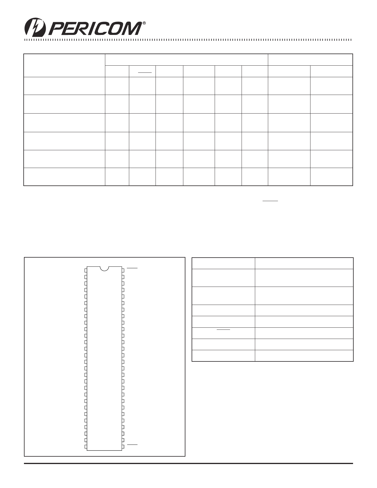
Product Pin Configuration
1OEAB
1CLKAB
1SAB
GND
1A0
1A1
VCC
1A2
1A3
1A4
GND
1A5
1A6
1A7
2A0
2A1
2A2
GND
2A3
2A4
2A5
VCC
2A6
2A7
GND
2SAB
2CLKAB
2OEAB
1
56
2
55
3
54
4
53
5
52
6
51
7
50
8
49
9
48
10
47
11
46
12
45
13 56-PIN 44
14 V56 43
15 A56 42
16
41
17
40
18
39
19
38
20
37
21
36
22
35
23
34
24
33
25
32
26
31
27
30
28
29
1OEBA
1CLKBA
1SBA
GND
1B0
1B1
VCC
1B2
1B3
1B4
GND
1B5
1B6
1B7
2B0
2B1
2B2
GND
2B3
2B4
2B5
VCC
2B6
2B7
GND
2SAB
2CLKBA
2OEBA
Product Pin Description
Pin Name
Description
XAX
Data Register A Inputs
Data Register B Outputs
XBX
Data Register B Inputs
Data Register A Outputs
xCLKAB, xCLKBA
Clock Pulse Inputs
SAB, SBA
Output Data Source Select Inputs
XOEAB, XOEBA
Output Enable Inputs
GND
Ground
VCC
Power
2
PS2094B 09/20/02
Share Link: 