CS-52845D14(1997) Просмотр технического описания (PDF) - Cherry semiconductor
Номер в каталоге
Компоненты Описание
производитель
CS-52845D14 Datasheet PDF : 6 Pages
| |||
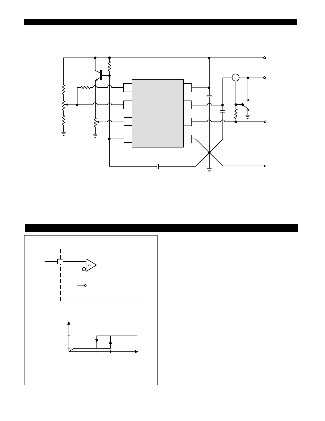
Test Circuit Open Loop Laboratory Test Fixture
4.7kW
1kW
Error Amp
Adjust
4.7kW
RT
2N2222
100kW
COMP
5kW
Sense
Adjust
VFB
Sense
OSC
VREF
VCC
V O UT
Gnd
CT
A
0.1mF
0.1mF
1kW
1W
VREF
VCC
V O UT
Gnd
Circuit Description
Undervoltage Lockout
During Undervoltage Lockout (Figure 1), the output driv-
er is biased to sink minor amounts of current. The output
should be shunted to ground with a resistor to prevent
VCC
ON/OFF Command
activating the power switch with extraneous leakage cur-
to reset of IC
rents.
VON = 8.4V
VOFF = 7.6V
ICC
<15mA
<1mA
VON VOFF
Figure 1: Startup voltage for the CS-52845.
PWM Waveform
To generate the PWM waveform, the control voltage from
the error amplifier is compared to a current sense signal
which represents the peak output inductor current (Figure
2). An increase in VCC causes the inductor current slope to
increase, thus reducing the duty cycle. This is an inherent
feed-forward characteristic of current mode control, since
the control voltage does not have to change during
changes of input supply voltage.
When the power supply sees a sudden large output cur-
rent increase, the control voltage will increase allowing
VCC
the duty cycle to momentarily increase. Since the duty
cycle tends to exceed the maximum allowed to prevent
transformer saturation in some power supplies, the inter-
nal oscillator waveform provides the maximum duty cycle
clamp as programmed by the selection of OSC compo-
nents.
4
Share Link: 