LP2950AC Просмотр технического описания (PDF) - Signal Processing Technologies
Номер в каталоге
Компоненты Описание
производитель
LP2950AC Datasheet PDF : 13 Pages
| |||
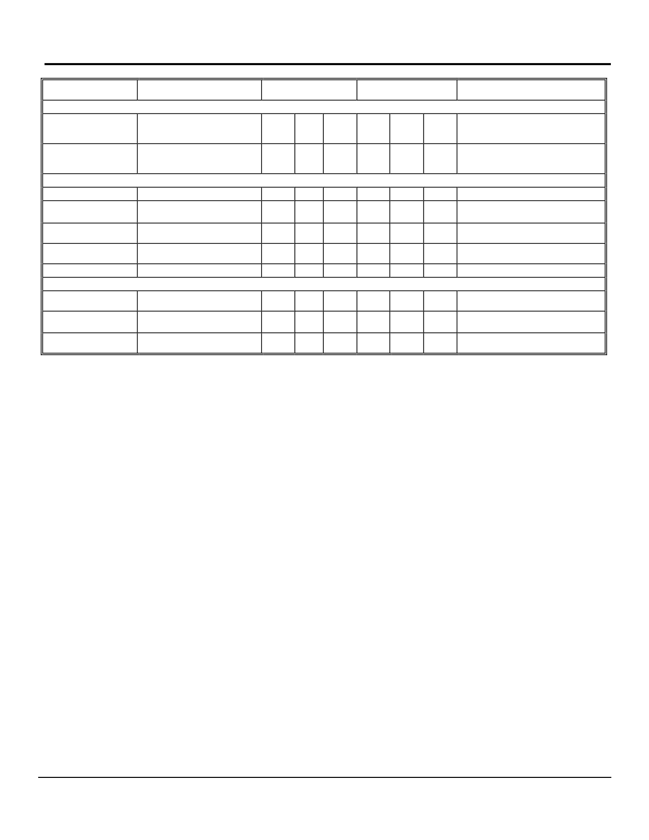
LP2950/51
CONDITIONS
PARAMETER
(Note 2)
8-Pin Versions only (Continued)
Reference Voltage
Temperature
Coefficient
Feedback Pin Bias
Current
Temperature Coefficient
Error Comparator
Output Leakage Current VOH = 30V
Output Low Voltage
Upper Threshold
Voltage
Lower Threshold
Voltage
Hysteresis
VIN = 4.5V
IOL = 400µA
(Note 7)
(Note 7)
(Note 7)
Shutdown Input
Input logic Voltage
Shut down Pin Input
Current
Regulator Output
Current in Shutdown
Low (Regulator ON)
High (Regulator OFF)
VS = 2.4V
VS= 30V
(Note 8)
LP2951AC
LP2951C
Min. Typ. Max. Min. Typ. Max.
20
50
0.1
0.1
0.01 1
150 250
0.01 1
150 250
40
60
40
60
75 95
75
95
15
15
1.3 0.7
1.3
0.7
2.0
2.0
30 50
675 800
30
50
675 800
3
10
3
10
UNITS
ppm/¡C
nA/¡C
µA
mV
mV
mV
mV
V
V
µA
µA
µA
Note 1: Output or reference voltage temperature coefficients defined as the worst case voltage change divided by the total temperature range.
Note 2: Unless otherwise specified all limits guaranteed for TJ = 25°C, VIN = 6V, IL = 100µA and CL = 1µF. Additional conditions for the 8-pin versions are feedback
tied to 5V tap and output tied to output sense (VOUT = 5V) and VSHUTDOWN ≤ 0.8V.
Note 3: Regulation is measured at constant junction temperature, using pulse testing with a low duty cycle. Changes in output voltage due to heating effects are
covered under the specification for thermal regulation.
Note 4: Line regulation for the LP2951 is tested at IL = 1mA. For IL = 100 µA and TJ = 125°C, line regulation is guaranteed by design to 0.2%. See typical
performance characteristics for line regulation versus temperature and load current.
Note 5: Dropout voltage is defined as the input to output differential at which the output voltage drops 100 mV below its nominal value measured at 1V differential. At
very low values of programmed output voltage, the minimum input supply voltage of 2V (2.3V over temperature) must be taken into account.
Note 6: VREF ≤VOUT ≤ (VIN - 1V), 2.3 ≤VIN≤30V, 100µA≤IL≤ 100mA, TJ ≤ TJMAX.
Note 7: Comparator thresholds are expressed in terms of a voltage differential at the feedback terminal below the nominal reference voltage measured at 6V input. To
express these thresholds in terms of output voltage change, multiply by the error amplifier gain = VOUT/VREF = (R1 + R2)/R2. For example, at a programmed output
voltage of 5V, the error output is guaranteed to go low when the output drops by 95 mV x 5V/1.235 = 384 mV. Thresholds remain constant as a percent of VOUT as VOUT
is varied, with the dropout warning occurring at typically 5% below nominal, 7.5% guaranteed.
Note 8: VSHUTDOWN ≥ 2V, VIN ≤ 30V, VOUT =0, Feedback pin tied to 5V Tap.
Note 9: All typical values are not guaranteed. The value could vary from lot to lot.
Rev. 8/10/01
LP2950/51 100mA Low Dropout Voltage Regulators
3
©Copyright 2001 Sipex Corporation
Share Link: 